Traffic Light Controller
Abstract
A controller for a European style traffic light was constructed using a simple finite state machine. The controller was built to learn about VHDL coding, CPLD programming, RAM timing and dealing with complexity in complicated projects. By using a "Keep it Simple" methodology, the complexity of the system as a whole was kept to a minimum, and resources were efficiently used. After an initial complexity nightmare, the device was built incrementally so that when errors did occur, their causes were easier to determine.
List of Figures
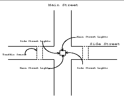
Street and traffic light arrangement 5
High level block diagram of the traffic light controller 9
FSM Block Diagram with synchronizer. 12
RAM data write timing diagram 14
Overview
The traffic light controller controls the red, yellow and green traffic lights for both streets in a simple intersection. One street is considered the main street and one is considered the side street. Both a walk button for pedestrians and a traffic sensor for the side street are included. When running, the lights are either in blink mode or they are in run mode. The time that each particular configuration of lights remains lit is programmable and can be between 1 and 15 seconds inclusive. The timing information is stored in a random access memory (RAM)). A user can examine the contents of the RAM by placing the device in the show memory mode.The user can set the timing parameters which are used to control the light interval using the store memory mode. The user can set four RAM locations (TBLINK, TYEL, TBASE and TEXT) corresponding to the four timing parameters.
Street and traffic light arrangement
When not setting or viewing memory, the traffic lights are either running or blinking. The transitions between states are accomplished by setting an internal countdown timer which asserts an expired signal after the specified number of seconds has elapsed. The expired signal triggers a finite state machine (FSM)) to go to the next state. When transitioning to the next state, the FSM selects which timing parameter to use, reads the parameter's value from the RAM and sets the countdown timer to count that many seconds and waits for the expired signal.
Blink Mode
When in blink mode, the traffic lights alternate between two states. The first state has the main street's red and side street's yellow light on. The next state has the side street's red light and the main street's yellow light on. The lights alternate between these two states every TBLINK seconds.
Run Mode
When in run mode, the traffic lights operate as a normal set of traffic lights in Europe. The difference between European traffic lights and American traffic lights is that just before a light turns from red to green, both the yellow and red lights are displayed for a short period of time. This time gives motorists a chance to start their cars if they have turned them off while waiting for their turn to go. The specific cycle of the lights is modified by both the walk button and the traffic sensor.
The lights begin with the main street showing green and the side street showing red for a period of TBASE + TEXT seconds. Then the main street shows yellow and the side street shows red and yellow for a period of TYEL. If the walk button has been pressed at any point during the current cycle, all of the traffic lights for both streets turn on for TEXT seconds to allow the waiting pedestrian to cross the street in safety. After the walk signal is finished or if the walk button was not pressed, the main street's light shows red and the side street's light shows green for a period of TBASE to allow waiting cars to go. If the traffic sensor reports that there are still cars on the side street after those TBASE seconds, the side street remains green and the main street stays red for an additional TEXT seconds. Afterwards, the side street's yellow and the main street's yellow and red lights are illuminated for TYEL seconds. Then the cycle repeats again.
The walk button can be pressed at any time in the cycle, but the lights only go into walk mode (all lights on) after the main street has been green. Pressing the walk button multiple times in a particular cycle has no additional effect.
The traffic sensor pulses as cars drive on and off of it, leading to the possibility of missing the signal when the FSM decides whether to keep the side street green for the additional TEXT seconds. With specialized circuitry, the controller keeps the sensor signal high for several seconds after a car has passed to avoid this pulsing problem.
Show Memory Location
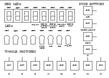
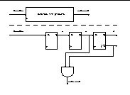
When the device is placed into show_memory mode, the memory data HEX LED shows the value stored in the RAM at the location specified by the memory location switches (see Figure 2).
Store Memory Location
When the go button is pressed, the value on the inputs c0,c1,c2,c3 are stored into memory at the location specified by l0,l1. The machine must be moved out of store memory location mode before one can program another memory location. This is accomplished by resetting the machine after the value has been successfully stored
Description
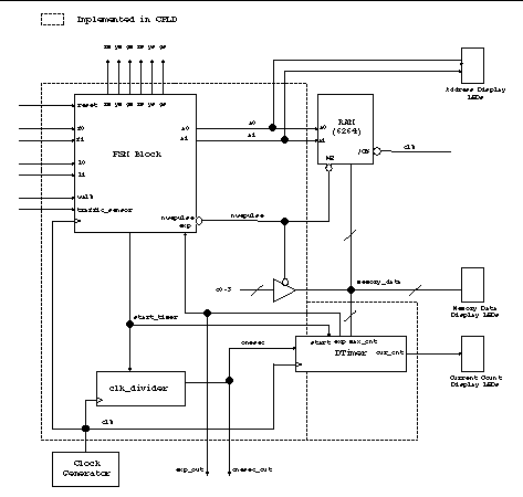
The five components of the traffic light controller were the finite state machine (FSM)), a RAM, a clock divider, a one second timer, and a count down timer. Figure 3 is the system block diagram. The FSM, one second timer and the count down timer were implemented using a single CPLD, a 6264 SRAM was used for storing timing parameters, and the clock divider was implemented with a crystal oscillator and a pair of `393 dual four bit binary counters. Each of the modules and its particular implementation is described below. Also included is why each implementation was chosen.
Finite State Machine
The FSM is responsible for coordinating activities among the different modules. In the system diagram in Figure 3, the FSM is contained inside of the FSM Block which handles synchronization of input and output signals. The synchronization hardware and implementation rationale is described in the FSM Block explanation below.
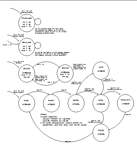
The state transition diagram in Figure 4 shows the details of the FSM's behavior, all possible states and the rules for transitioning from one state to the next.
FSM Block design
The FSM has 11 states and is not overly complicated. All of the transition arcs are triggered by the reset signal, the go signal, or the expired signal. If reset is ever pressed, the controller returns to the show memory mode. If go is pressed, the controller goes to the mode specified by inputs f0 and f1. If the controller is in either blink or run mode, the expired signal causes the transition to the next state of lights. Because the FSM was kept to such a small number of states, timing issues dominated its design.
To avoid corrupting the timing data stored in RAM, the write enable for the RAM must be active for only one clock pulse while the data and address have stabilized (see the RAM section below for a timing diagram). Also, the write enable pulse should occur for only one clock cycle to avoid corrupting the RAM by allowing the input data to change. One possible strategy is to introduce three states in the FSM for writing to RAM. One state would be responsible for setting the address and data, the next for asserting the write enable signal and the final state to unassert the write enable signal. This approach was discarded because it introduced unnecessary complexity into the FSM.
In place of multiple states, a special synchronizer (Figure 5) circuit was constructed which both delays the write enable signal and asserts it for exactly one clock cycle. The FSM can then assert the write enable signal for as long as it is in the store_mem state and not worry about corrupting the RAM because the write enable signal the RAM receives will only be active for a single clock period. The disadvantage to this design is that resetting the leveltopulse circuit requires the write enable to be reset, and this requires the FSM to be taken out of store_mem mode. Taking the machine out of store memory mode is most easily accomplished by using the reset button to move the FSM to the show memory mode.
Leveltopulse circuit
Using this design, the user is more likely to get confused because of the need to reset the machine between writes, but the overall system complexity is less. However, programming timing parameters is not a common operation. Instead of simplicity in programming, simplicity in design tends to make systems more reliable. The extra time necessary to learn the controller's programming procedure is not an undue burden because of its rarity, and the additional reliability introduced is worth the trade-off.
While in run or blink mode, the FSM goes to the next state when the expired (exp) signal is asserted. The FSM sets the RAM address (a1a0) to the address for the next state (e.g. TBLINK, TYEL, TEXT or TBASE), and asserts the start_timer signal. The start_timer signal tells the countdown timer (DTimer module) to save the value the RAM is currently writing to the memory_data bus and begin counting. When the DTimer has counted to the specified value, it asserts the expired signal, causing the cycle to be repeated.
It takes a full clock cycle after the address has been asserted for the RAM to place the correct value on the memory_data bus. If both start_timer and the address were asserted on the same cycle, the value saved by the count down timer would be the RAM's contents at the previously asserted address. Hence, start_timer needs to be asserted one cycle after the address is asserted.
One possible approach that was discarded was three states in the FSM for each transition. One state would be to set the address, another to start the timer, and a third to wait for the expired signal. This design would increase the number of states required by a factor of three, and hence was not acceptable due to the goal of design simplicity.
Instead of multiple states for each traffic signal, a one clock cycle delay was placed on start_timer between the FSM and the DTimer using the leveltopulse circuit. This gives the RAM a cycle to prepare the appropriate output before starting the timer, and keeps the start_timer signal from being asserted multiple times and thereby resetting the timer continuously.
FSM Block Diagram with synchronizer.
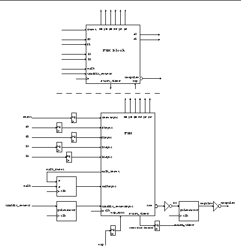
Events in the real world such as pressing the walk button and setting function switches do not happen synchronously to the system clock. Hence, all user input was synchronized before being used as inputs to the FSM to avoid unwanted transitions.
The switch input from the signals f0,f1,a0,a1 and reset were synchronized using D flip flops to ensure valid data at the rising edge of each clock cycle. The go signal was synchronized using the same leveltopulse circuit that the write enable pulse used. The leveltopulse circuit ensures that the go signal is asserted for only one clock cycle every time it is pressed. The signal from the traffic sensor was synchronized using the pulsesaver circuit (Figure 7) which remains high for several cycles after its input has been asserted. The traffic sensor signal was saved so that if a car had happened to have just rolled off of the sensor before the next one rolled on, and the FSM was deciding to give the side street more time with the green light, the traffic_sensor input would still be asserted and the FSM would give the side street the additional time.
Pulsesaver circuit
The walk button is a special case of user input. A walk request is only handled at a single point in the traffic light cycle. When a user presses the walk button, the traffic light controller needs to remember that it was pressed even though the request might not be handled until several transitions later. An SR latch was used to save the pedestrian's request. After the FSM has successfully serviced the walk request, it resets the latch via the walk_reset signal. Figure 6 shows all of the synchronization circuitry within the FSM Block.
Table 4 summarizes all of the outputs and state encodings of the FSM.
RAM
A 6264 RAM was used to store the timing data. The RAM's address bus was run by a CPLD output and hence was susceptible to glitches. If the address changes while the RAM is reading, the RAM could retrieve the wrong data. To ensure that the address asserted did not change during a write pulse, the /CS (Chip Select) was wired to the clock. Since the actual data write occurs when both the /WE (write enable) and /CS are low, the address output from the CPLD has half a clock cycle to stabilize before the RAM was allowed to write. Because the system clock is fairly slow (see the clock divider section), a half cycle clock delay was plenty of time for the address output to stabilize.
RAM data write timing diagram
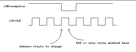
Similar timing issues are involved in reading data from the RAM. The RAM's address must be held stable for a period of time before any data can be read from its data port. As explained in the FSM section, the FSM asserts the data address a full clock cycle before data was read from the RAM. The extra cycle allowed the RAM enough time to present the data corresponding to the new address on the memory_data bus.
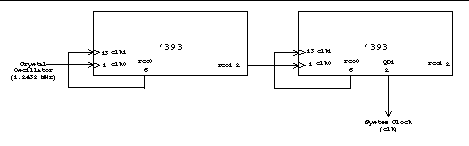
Clock Divider and One Second Timer
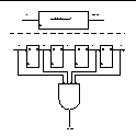
The one second timer's function was to assert a signal, onesec, every second. A 1.8432 MHz crystal oscillator was used as the base timer for the system. 1.8432x10⁶ pulses from the crystal occur every second.
One second generator block diagram
One simple solution for the one second timer is to create a 21 bit counter using a CPLD and count up to 1.8432x10⁶ from 0. This takes a lot of CPLD resources because the compiler attempts to make the fastest 21 bit counter possible. In similar designs which used this method, it was necessary to use a separate CPLD to accommodate the one second timer in addition to the CPLD used to accommodate the FSM and countdown timer.
Since the goal of this design was simplicity, adding another CPLD to the design was unacceptable. Instead, by noticing that 1.8432x10⁶ is 11100001000000000000 in base 2, the first 13 bits of counting can be done outside of the CPLD. It is not necessary to have a very fast system clock since the machine only has to transition at most once a second. Doing the first 13 bits of division externally, the system clock ran at 1.8436/213 MHz.
To accurately time a second, the one second timer module counts up to 11100001 in binary, asserts the onesec signal and then resets its internal counter. When the start_timer is asserted by the FSM, the internal counter is also reset. This reset is done so that the onesec pulses are generated every second starting from when the start_timer was asserted.
Two `363 dual 4 bit binary counters were used to perform the first 13 bits of clock division. Four counter modules were used, and the 13th bit as shown in Figure 9 was used as the system clock.
Countdown timer (DTimer) block diagram
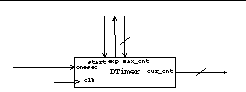
The countdown timer was implemented in VHDL and then programmed into the main CPLD. The timer waits until it receives a start signal, at which point it latches its max_cnt input, resets its internal counter, and begins counting every second. The current count is passed to the output cur_cnt so the user could observe the current time. The countdown timer is clocked with the main system clock, but its internal counter is only enabled when the onesecond signal is asserted, and hence it only counts once a second. The onesecond signal comes directly from the clock divider module explained above. When the internal counter is equal to the stored max_cnt, the countdown timer asserts the exp signal and stops counting. By asserting the expired signal, the DTimer causes the FSM to transition to the next state.
Testing and Debugging
Because traffic light controllers are something that I took for granted in my daily life, originally this project seemed very simple. I programmed my FSM in VHDL, ran extensive simulations, was satisfied that it worked the way that I wanted and burnt the resulting file on to a CPLD. I powered it up and (not surprisingly) it did nothing. I had no idea what the problem was or even where to begin looking for a solution. The lesson I learned was to build the system incrementally. That way, when something doesn't work, you have made only a small number of changes that could be responsible. I adopted this strategy and set about creating the traffic light controller.
I started debugging by first sitting down with my VHDL code and setting the pin assignments to the user interface specified above. While the CPLD has many connections in the lab kit, the VHDL compiler does not know anything about them. The results of this spending a lot of time programming pin numbers was that I could see exactly what state the FSM was in any particular time, and get an idea as to what was happening internally.
Then, I removed the FSM entirely from the design, and focused on getting the timing working correctly. I spent quite a while before realizing that the ribbon cable that connects the CPLD board to the lab kit via the K1 interface does not work if you plug it in backwards. After I got past that glitch, and I had visual confirmation that my one second timer was working (via LED0 flashing) I moved onto the FSM.
I gutted the majority of the VHDL code for the FSM, leaving only the save_mem and show_mem states. After making some procedural mistakes such as programming the CPLD without disabling the clock, I got the basic FSM to change states by pressing the reset and the go buttons. Once I was satisfied that the write enable and the start_timer signals were being correctly asserted, I connected the RAM. I wired the RAM to the appropriate signals, and hooked up the data switches to the memory busses using tristate drivers in a `244 chip. To my surprise and great relief, when I tried to store data to the RAM, the controller worked on the first try.
With the show_mem and store_mem states working, I added the code for the two blink states back into the FSM. If I could get the controller to blink, I would know that the DTimer module was counting down and exerting the expired signal correctly. When I first inserted the code, it did not work because the expired signal was continually asserted. When the expire signal was asserted, the FSM could not restart the timer because to asserting the start timer signal required that the expired signal be unasserted. I inserted the leveltopulse circuitry between the timer and the FSM (as described above) to fix the problem. With that fix, I had a blinking traffic light.
Then, I added in the main signal sequence still leaving out the go and walk states. Since I had gotten the blink sequence to work correctly, I expected the main sequence to work as well, and it did on the first try. Then I restored my original tested VHDL code for dealing with walk requests, recompiled, and reprogrammed the CPLD. Happily, the walk button functionality also worked on the first try. Then I recompiled again, adding back the traffic sensor functionality. It also worked on the first try. I believe that these additions worked on the first try because I had already dealt with all of the timing bugs in previous debugging and I had initially thought about and designed for synchronization issues. However, by implementing the design incrementally, I could ensure that I had the basic timing issues solved before adding more complicated functionality.
I had a working traffic light, and I was about to try to get it checked off by a TA when I noticed that the behavior was not quite right. The timer was counting correctly, but the value that it was counting up to was the value specified for the previous RAM location. After thinking about this for a while, I realized that the DTimer was latching the value on the memory bus the same cycle that the address was being asserted. Furthermore, the RAM didn't actually write data to the bus until the last half of the cycle when the clock signal was low because the /CS line was wired to the system clock. Hence, I needed to delay the starting of the count down timer for one cycle to give the RAM time to write the correct value onto the memory data bus. By adding a D flip flop in the FSM block, I fixed the bug.
Conclusion
The design for the traffic light controller had simplicity as its goal. By using introducing simple circuitry to delay signals as they traveled though the system, many FSM states to setup the RAM were avoided. By moving a large portion of the clock division into external counters, the VHDL code was smaller, simpler and fit on one CPLD. Since all of the design fit onto one CPLD, the complexity in using two CPLDs was avoided. An implementation methodology of incremental addition, adopted after an original complexity nightmare, served well to keep errors localized and easy to correct.
Appendices
CPLD Macrocell Utilization
Information: Macrocell Utilization.
______________________________________
| Buried Macrocells | 25 | 64 |
| PIM Input Connects | 88 | 312 |
______________________________________
CLOCK/LATCH ENABLE signals 1 4
D Flip Flop VHDL Code
-- This comment is before the library and use clauses.
SR Flip Flop VHDL Code
-- This comment is before the library and use clauses.
-- a JK type flip flop triggered on the rising edge of the clock
architecture comp of myjkff is
signal jkff : std_logic := `0';
Leveltopulse VHDL Code
-- This comment is before the library and use clauses.
port (levelin,clk : in std_logic;
-- here is the architcture (from lecture 7 notes)
architecture comp of leveltopulse is
signal x,y,z : std_logic; -- internal signals for flip
-- now make the final little bit o' logic which
Pulsesaver VHDL Code
-- a componenet to assert a level for at least 4 cycles after the pulse has
architecture comp of pulsesaver is
signal w, x, y, z : std_logic;
-- if any of these saved levels(w,x,y,z) are high, then the output is high
FSM VHDL Code
-- This comment is before the library and use clauses.
port (resetsync, l0sync, l1sync, f0sync, f1sync : in std_logic;
gosync, auxsync, walk_request, exp, clk : in std_logic;
state_out : out std_logic_vector(3 downto 0);
a0, a1, nwe, start_timer,walk_reset : out std_logic;
rm, ym, gm, rs, ys, gs : out std_logic);
architecture state_machine of fsm is
-- rmgs = red main, greed side (so red on the main street, green on the side
type StateType is (mrsg, mrysy, mgsr, mysry, walk,
blink1, blink2, mrsg_ext, mgsr2);
attribute enum_encoding of StateType:
type is "0000 0001 0010 0011 0100 0101 0110 0111 1000 1001 1010";
-- figure out which state to goto next
-- 1. Only do things on a rising clock edge
-- 2. if reset is asserted, goto state show_mem
-- if gosync is asserted, the user has requested action, so set mode
-- based on functions selected (f0sync and f1sync).
-- if expired is asserted, then goto the next state in the run cycle
-- otherwise, stay in the same state
state_transition:process(exp, resetsync, gosync, f1sync, f0sync, p_s, auxsync, walk_request)
-- check reset signal, and set to show_mem state
-- change the machine to one of the four predefined states
-- 10 start the normal operation of the lights (in green main,
if ((f1sync = `0') and (f0sync = `0')) then
elsif ((f1sync = `0') and (f0sync = `1')) then
elsif ((f1sync ='1') and (f0sync = `0')) then
walk_reset <= `1'; -- reset the walk signal initially
elsif ((f1sync = `1') and (f0sync = `1')) then
if walk_request = `1' then -- if we are waiting for a walk request
walk_reset <= `1'; -- reset the walk latch
if auxsync = `1' then -- some cars are waiting still
n_s <= p_s; -- by defaut, say in the same state
n_s <= p_s; -- by default, STAY IN THE SAME STATE
nwe <= `0' when n_s = store_mem else `1';
state_out(0) <= `1' when ((p_s = mrysy) or
state_out(1) <= `1' when ((p_s = mgsr) or
state_out(2) <= `1' when ((p_s = walk) or
state_out(3) <= `1' when ((p_s = blink2) or
rm <= `1' when ((p_s = store_mem) or
ym <= `1' when ((p_s = blink1) or
gm <= `1' when ((p_s = store_mem) or
rs <= `1' when ((p_s = show_mem) or
ys <= `1' when ((p_s = blink2) or
gs <= `1' when ((p_s = show_mem) or
a1 <= `1' when ((l1sync = `1' and p_s = store_mem) or
(l1sync = `1' and p_s = show_mem) or
a0 <= `1' when ((l0sync = `1' and p_s = store_mem) or
(l0sync = `1' and p_s = show_mem) or
end architecture state_machine; --"architecture" is optional; for clarity
FSM Block VHDL Code
entity userinput_synchronizer is
l0sync,l1sync : out std_logic;
f0sync,f1sync : out std_logic;
go,traffic_sensor : in std_logic;
gosync,auxsync : out std_logic;
architecture arch of userinput_synchronizer is
process(clk,l0,l1,f0,f1,reset,go,traffic_sensor)
---now add in a level to pulse for the go
--now, save the traffic sync for a few clocks
use work.userinput_synchronizer;
-- the fsm_block is an organizational unit for
-- setting up all of the appropriate synchronization
port (reset, l0, l1, f0, f1 : in std_logic;
go, traffic_sensor : in std_logic;
state_out : out std_logic_vector(3 downto 0);
a0, a1, nwepulse, start_timer : out std_logic;
rm, ym, gm, rs, ys, gs : out std_logic);
architecture arch of fsm_block is
signal resetsync, l0sync, l1sync, f0sync, f1sync : std_logic := `0';
signal gosync, auxsync : std_logic := `0';
-- write enable signals (so we can catch a level and convert to a pulse)
signal we,wepulse : std_logic := `0';
signal nwe : std_logic := `1';
signal walk_request_latched : std_logic := `0';
signal walk_clear : std_logic := `0';
-- internal sart timer signal so that we can make sure that the ram has
-- read out the data before we start the timer
signal start_timer_internal : std_logic;
-- set up the user input synchronizer
UISYNCER : userinput_synchronizer
traffic_sensor => traffic_sensor,
-- wire up a synchronizer from the write enable line of the fsm
-- to the actual write enable strobe from the fsm_block
-- set up a jk flip flop on the walkrequest input
walk_request => walk_request_latched,
start_timer => start_timer_internal,
--now, catch the start timer signal with a d flip flop to delay it another
DTimer VHDL Code
-- the D-Timer for the traffic light controller.
-- This logic block is used as a counter. It counts from
-- 0 to some specified number and the asserts the exp signal.
-- when start is asserted, the max_cnt is loaded.
-- when the counter output = max_cnt, then exp is asserted and
port (start, clk : in std_logic;
max_cnt: in std_logic_vector(3 downto 0); -- the max count
cur_cnt: out std_logic_vector(3 downto 0);
exp : out std_logic); -- expired signal
architecture comp of dtimer is
signal cur_max : std_logic_vector(3 downto 0);
signal cur_cnt_int : std_logic_vector(3 downto 0);
process (clk, start, max_cnt, onesec)
cur_max <= max_cnt; -- save the max_cntimum
cur_cnt_int <= "0000"; -- reset the count
if not (cur_cnt_int = cur_max) then
cur_cnt_int <= cur_cnt_int + 1; -- increment count
-- the exp signal is asserted when count equals max_cnt
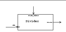
Divider (one second generator) VHDL Code
use work.std_arith.all; -- so we can use `+'
-- a clock divider for the generating the 1/sec pulses
architecture comp of divider is
signal cnt : std_logic_vector(7 downto 0);
if start = `1' then -- if we are starting, reset the count
cnt <= (others => `0'); -- start counting again
cnt <= (cnt + 1); -- increment the count
CPLD Chunk Code (top level entity)
-- set up the top level CPLD layout
cur_cnt : out std_logic_vector(3 downto 0);
mem_data : in std_logic_vector(3 downto 0);
current_state : out std_logic_vector(3 downto 0);
rm,ym,gm : out std_logic; -- main street lights
rs,ys,gs : out std_logic); -- side street lights
ATTRIBUTE pin_avoid of cpld_chunk :ENTITY is
-- " 1 2 11 21 22 32 42 43 44 53 63 64 74 83"& -- Vdd, Gnd, VPP
" 12 19 73 "& -- These pins are the interconnect bus
-- for CPLD 2, 3, and 4. They are Serial I/O
" 13 "& -- This is I0-9. Can screw up the clock of C1. Be
-- The CPLD has 4 clock pins that can also be used as input pins.
-- However, all of them are tied together.
-- The 4 clock pins are " 20 23 62 65 " .
-- Depending on your design, the programmer will assign of them
-- to be the clock input, and use the others as general-purpose inputs.
-- This can be quite frustrating.
-- We will thus disable 3 of the 4 and hope the compiler likes our
-- choice. If it doesn't, we will just have to pick another one.
-- Lets use clock 1 and disable clock 2,3, and 4.
-- If we need to use clock 2 : then use " 20 62 65 "&
-- If we need to use clock 3 : then use " 20 23 65 "&
-- If we need to use clock 4 : then use " 20 23 62 "&
" 14 35 41 51 72 " & -- Used by Programmer. No external connection.
" 30 31 36 37 40 45"; -- hibits of the hex leds
attribute pin_numbers of cpld_chunk:entity is
"cur_cnt(0):46 cur_cnt(1):47 cur_cnt(2):48 cur_cnt(3):49 " &
"mem_data(0):24 mem_data(1):25 mem_data(2):26 mem_data(3):27 " &
"current_state(0):8 current_state(1):10 current_state(2):18 current_state(3):68 " &
"go:3 reset:4 traffic:5 walk:6 " &
architecture arch of cpld_chunk is
-- sync exp signal to system clock
-- instantiate the fsm (dear god)
-- pass ome interesting signals out so we can view them externally