6.111 Lab 3
Abstract
A device that shifts the pitch of an input sound signal is presented in detail. The pitch shifter uses a simple algorithm of stretching or squeezing a sample in time to perform the desired pitch shift. The system's Analog to Digital and Digital to Analog mechanisms are examined in detail. The system also includes a Micro-Programmable Control Unit, whose instruction format and operation are explained. A Storage Unit for addressing the necessary buffers and an Accumulator for mixing the original and shifted signals are also presented. A major problem in the Accumulator that was encountered is described and a work around of the problem is presented. Finally, some reflections on lessons learned are discussed.
Table of Contents
Block diagram and input specification 5
Digital portion of the pitch shifter 7
Input (Analog to Digital conversion) 10
Accumulator and Output (Digital to Analog conversion) 21
Debugging Strategy and Experience 27
MCU checkoff: make a detailed diagram 27
List of Figures
System diagram without analog signals 7
Pitch shifter system block diagram 8
Relative size of the sample clock and system clock 9
Timing unit code (timingunit.vhd) 9
MCU hardware implementation 12
Flow control diagram for pitch shifter 13
Specification file (mcu.sp) 14
Block diagram of storage unit 16
Relation of increment signal to shift buffer address 17
Pitch Multiplier Counter (pitchmultipliercounter.vhd) 17
Storage Unit (storageunit.vhd) 20
Accumulator VHDL(accumulator.vhd) 22
VHDL code for 22V10 accumulator flip flop(8bitreg.vhd) 25
External synchronization circuit 26
MCU test specification file (mcutest.sp) 27
Introduction
For the third laboratory experience in 6.111, a sound pitch shifter was built. The pitch shifter takes as an input an analog voltage representing a sound wave, and produces as an output an analog voltage representing a pitch shifted version of that sound. The shifted signal can have either higher or lower pitch than the original signal. The output can be either one or an arithmetic average of the original signal and the pitch shifted signal.
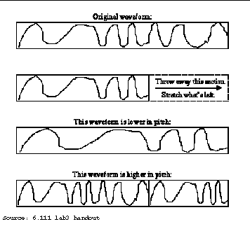
To produce the pitch shift, short samples of the input are recorded. The samples are then played back either faster or slower than they were recorded. By playing the sample back slower than it was recorded, the perceived pitch is shifted down. By playing the sample back faster that it was recorded, the perceived pitch is shifted up. To stretch out the sample, the information at the end of the sample is discarded. To squish the sample, some of the sample's information is played twice. Figure 1 illustrates how a particular sample's pitch can be modified by stretching or squishing the original waveform.
Overview
Block diagram and input specification
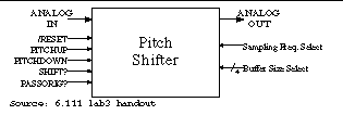
A block diagram for the entire system is given in Figure 2. The user interface and inputs are listed in Table 1.
Total system block diagram
A/D and D/A considerations
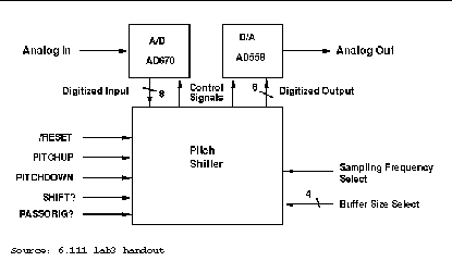
By removing the analog signals from the block diagram, the design of the pitch shifter can be done exclusively in the digital domain. The separation of the analog components from the digital components is shown in Figure 3.
The A/D is an Analog to Digital converter. The A/D is a single chip which converts an instantaneous analog voltage on its input line into an 8 bit digital value on its output lines. The time at which the A/D samples the input voltage is determined by control signals generated by the digital pitch shifter.
The D/A block is a Digital to Analog converter. The D/A is a single chip which converts a 8 bit digital value on its input lines into an analog voltage on its output lines. In this implementation of the pitch shifter, the D/A is a part of the Accumulator, and hence the digital part of the pitch shifter only deals with the D/A indirectly through the Accumulator interface.
Digital portion of the pitch shifter
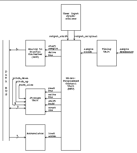
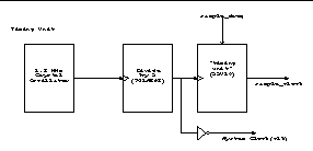
Figure 4 illustrates the further decomposition of the pitch shifter into its component modules. The heart of the pitch shifter is a Micro-Programmed Control Unit (MCU). An MCU is similar to the CPU found in personal computers, except that the MCU is specialized to a particular task. The MCU has specialized output for controlling the A/D, the Storage Unit, and the Accumulator. The MCU is programmed using an assembly language created specifically for the pitch shifter system and that is described in detail below.
In addition, the pitch shifter also contains a Timing Unit which provides both the system clock and the sample clock. The sample clock determines the rate at which the pitch shifter samples the input signal. The frequency of the sample clock depends on the current setting of the sample_frequency input switch.
The Storage Unit is responsible for maintaining two buffers using a Random Access Memory (RAM). The sample buffer is filled with the current sample. The shift buffer contains the last sample recorded. By reading the shift buffer either more or less quickly than the sample buffer, the pitch of the stored sample can either be increased or decreased.
The Accumulator allows a mixture of the original and the shifted signal to be outputted at the same time. The Accumulator can average its current value with a new value to easily mix the two signals together.
Timing Unit
Overview
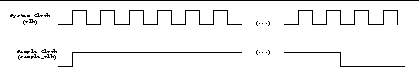
The Timing Unit uses a 1.8 MHz clock from a crystal oscillator to produce a 900 KHz system clock and either 19.2 KHz or 9.6 KHz sample clock. A block diagram of the Timing Unit is shown in Figure 5.
System clock
The system clock is created by dividing the crystal clock in half by using a 74LS393 counter. The crystal oscillator is fed into the clock input of the 74LS939 and the second least significant bit of the output is used as a system clock. The output of the 74LS393 is buffered using a 74LS04 inverter to avoid clock skew. Clock skew is a potential problem because the system clock is widely distributed around the pitch shifter.
Sample clock
The sample clock is generated by using a 22V10 Programmable Array Logic (PAL) programmed with the VHDL code shown in Figure 7. Depending on the value of the sample_frequency input, the 22V10 produces a sample clock of 9600 Hz or 19200 Hz clock on its output. It is important to note that the sample clock is much longer than the system clock. The relative length of the sample clock to the system clock is shown in Figure 6.
Timing unit code (timingunit.vhd)
-- this is the timing usint which creates
-- a 9600 Hz signal on sampout if sampspeed is 0
-- or a 19.2 kHz signal if sampspeed is 1
attribute pin_numbers of timingunit:entity is
architecture timingarch of timingunit is
signal int_cnt : std_logic_vector(5 downto 0);
-- out counting process counts to 96 (110000) and then resets
if (int_cnt = "110000" and sampspeed = `1') then
int_cnt <= (others => `0'); -- reset timer if fast samp speed
int_samp <= not int_samp; -- cause the timer to oscillate
elsif (int_cnt = "011000" and sampspeed = `0') then
Input (Analog to Digital conversion)
The conversion of the input analog signal to a digital signal that the pitch shifter can manipulate is done using the AD670 8-bit ADC made by Analog Devices Corporation. Once the AD670 has been signaled to sample, it takes approximately 10 microseconds to perform a conversion. After 10 microseconds, the data representing the sample from the AD670 can be written to the output pins by sending the AD670 appropriate control signals. A timing diagram for the conversion cycle used in the pitch shifter is shown in Figure 8.
A/D timing
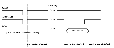
The conversion cycle is started by pulsing both the R/n_W and the n_CE/n_CS lines low. The conversion is finished a maximum of 10 microseconds later. The output pins are in a high impedance state until the n_CE/n_CS line is brought low. A few nanoseconds later, the AD670 drives the output pins with an 8 bit value representing the input voltage.
MCU
Overview
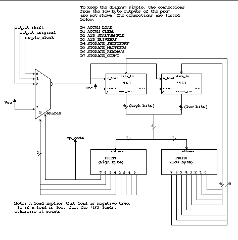
The MCU controls the operation of the pitch shifter by asserting various control signals to the other modules. The MCU is created from two 28F256A (8 bit address, 8 bit data word) Programmable Read Only Memories (PROMs). When composed together, the two PROMs create 16 bit instructions at each 8 bit address.
If the instruction at the current address asserts control signals, the MCU will execute the instruction at the next address on the following clock cycle. If the instruction at the current address is a jump, the MCU executes the instruction at an address specified in the current instructions data. Jumps may be conditional (CJMP) or unconditional (JMP). Conditional jumps only occur if a certain condition (such as the sample clock currently being high) is true. Unconditional jumps always force the MCU to jump to a new instruction because their condition (0b111) is wired high and hence always true.
MCU instruction format
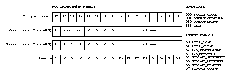
Figure 9 shows the instruction format of each 16 bit MCU instruction. The most significant bit of the instruction is the opcode. If the opcode is a 1, the instruction is called an ASSERT instruction. In each ASSERT instruction, the low 8 bits of the instruction control signals to rest of the pitch shifter. More than one control signal may be asserted in each ASSERT instruction. If the opcode is a 0, the instruction called a CJMP instruction. When executing a CJMP instruction, the MCU compares the value at the conditional address specified by bits 14 through 12 of the instruction. If the condition value is high (logical true) the next instruction that the MCU executes is the address specified in the lowest 8 bits of the instruction. If the conditional value is false, the MCU executes the instruction at the next address.
Hardware implementation
The hardware to implement the MCU is shown in Figure 10. The two 74LS163 counters keep track of the current instruction being executed. If the opcode is a 0b0, then the conditional mux is enabled. The input that the conditional mux selects is specified by the conditional address, located in bits 14 through 12 in the instruction. If the condition selected is high, the 74LS163s are loaded with the value contained in the last 8 bits of the instruction.
If the opcode is 1, then the last 8 bits in the instruction are interpreted by the rest of the pitch shifter as control signals.
Flow control
Figure 11 shows a flow chart representing the MCU program in the pitch shifter. Figure 12 shows the assembly specification file for the MCU, and Figure 13 shows the actual assembly which implements the pitch shifter.
Flow control diagram for pitch shifter
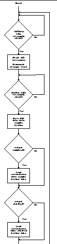
The MCU is in an infinite loop which begins by looking for the falling edge of the sample clock. When the falling edge of the sample clock occurs, the MCU signals the A/D to take a sample and the Storage Unit to increment the current count.
The A/D can't be read from until it has finished converting the sample. Instead of querying the A/D, the MCU assumes that the sample clock is so long compared to the A/D conversion time by the rising edge of the sample clock, the sample may be read with impunity.
The RAM used in the storage unit is sensitive to changes on its address lines. Even worse, the address lines are controlled by a Cypress 374I CPLD (Complex Programmable Logic Device) which has glitchy outputs. To avoid errors due to changing address lines during a read or write to or from the RAM, the address count is incremented a long time before any RAM access is attempted. The MCU then waits for the rising edge of the sample clock to proceed.
On the rising edge of the sample clock, the current value is read from the A/D into the sample buffer of the RAM. If the user wishes the original signal to appear on the output, the MCU loads the accumulator with the newly written contents of the sample buffer. If the user wishes the shifted signal to appear on the output, the MCU tells the Storage Unit to address the shift buffer, and the MCU loads the accumulator with the data from the shift buffer.
Specification file (mcu.sp)
/* Specification file (modified from original given) */
/* created 3-7-98, modified 4-1-01 AAL */
/****************************************************************/
/* Instruction Word Organization: */
/* conditional branches 0cccxxxx aaaaaaaa */
/* unconditional branches 0111xxxx aaaaaaaa */
/* assertion statements 1sssssss ssssssss */
/* where c = status selection */
/* a = alternative address, i.e. jump address */
/****************************************************************/
op <15:0>; /* Indicates the available bits */
address op <7:0>; /* Indicates bit locations for addresses */
* Instruction set for your MCU
CJMP op<15>=%b0; /* Conditional JuMP */
JMP op<15:12>=%b0111; /* unconditional JuMP */
ASSERT op<15>=%b1; /* unconditional ASSERT */
/* These are defined so that you may use them to make your code more
* readable. Their use is not required, but it is helpful */
TRUE op<14:12>=%b111; /* This forces a true output of the 151 */
RESET op<15:0>=%b0111000000000000;
ACCUM_LOAD op<0>=1; /* asserted all of _next_ clock cycle */
ACCUM_CLEAR op<1>=1; /* asserted all of _next_ clock cycle */
A2D_STARTSAMPLE op<2>=1; /* asserted all of _next_ clock cycle */
A2D_DRIVEBUS op<3>=1; /* asserted all of _next_ clock cycle */
STORAGE_SHIFTBUFF op<4>=1; /* latched on the _next_ rising edge */
STORAGE_WRITEBUS op<5>=1; /* asserted all of _next_ clock cycle */
STORAGE_READBUS op<6>=1; /* asserted all of _next_ clock cycle */
STORAGE_COUNT op<7>=1; /* latched on the _next_ rising edge */
Assembly file (mcu.as)
/* created 3-1-98, modified 4-1-01 */
# SET_ADDRESS = 0; /* start at addr 0 */
BEGIN: IF SAMPCLK CJMP BEGIN; /* wait until sampclk falls low */
ASSERT A2D_STARTSAMPLE A2D_DRIVEBUS STORAGE_COUNT; /* start a sample cooking */
CLKWT: IF SAMPCLK CJMP DOCONV;
JMP CLKWT; /* now wait until sample clock goes high */
DOCONV: ASSERT ACCUM_CLEAR; /* clear the accumulator */
ASSERT A2D_DRIVEBUS; /* start the a2d outputting */
ASSERT A2D_DRIVEBUS STORAGE_READBUS; /* save the a2d output to ram */
IF OUTPUT_ORIGINAL CJMP OUTORIG; /* if we are supposed to be outputting the original signal */
JMP AORIG; /* jump to after orignal outputting */
OUTORIG: ASSERT STORAGE_WRITEBUS ACCUM_LOAD; /* data is valid last half of the clock cycle */
ASSERT STORAGE_WRITEBUS ACCUM_LOAD; /* Load accumulator with sample buffer data */
AORIG: IF OUTPUT_SHIFT CJMP OUTSHFT; /* test to see if we are to load the shifted signal */
JMP FINISH; /* nope, so we are done */
OUTSHFT: ASSERT STORAGE_SHIFTBUFF; /* get the RAM address stable */
ASSERT STORAGE_SHIFTBUFF STORAGE_WRITEBUS ACCUM_LOAD; /* prep for writing to accumulator */
ASSERT STORAGE_SHIFTBUFF STORAGE_WRITEBUS ACCUM_LOAD; /* load accumulator with shifted sample */
Storage Unit
Overview
The Storage Unit is responsible for generating the RAM addresses of the current sample and shift buffers. The Storage Unit addresses the sample buffer by default, but when the shift_buff signal is asserted, the Storage Unit addresses the Shift Buffer. The MCU does not worry about keeping track of buffers, maximum buffer sizes, or swapping the buffers. All of the book keeping is done internally by the Storage Unit. A block diagram of the Storage Unit is shown in Figure 14.
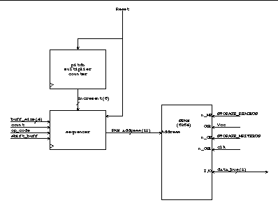
Buffer addressing
The sample buffer and the shift buffer are each comprised of 2048 (11 bits of address) locations with 8 bits of data each. A twelfth address bit is used to distinguish between the two buffers. Hence, a total of 4096 locations out of a possible 8192 in the RAM are used. When the sample buffer is full, the roles of the two buffers are swapped by reversing the twelfth address bit.
The pitch multiplier counter's 6 bit increment is used to increment the shift buffer's address. The increment is added to an internal 15 bit counter, and the top 11 bits of this internal counter are used as the shift buffer address. Pressing the shift_up button causes the increment to be increased, and pressing the shift_down button causes the increment to be decreased.
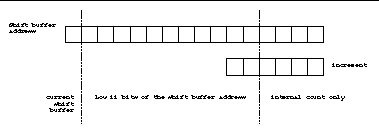
When the increment is 0b010000, the shift buffer address is the same as the sample buffer address (except for the twelfth bit) and the shifted signal is the same as the sampled signal. When the increment is greater than 0b010000, some shift buffer addresses are skipped. By skipping shift buffer addresses, the signal is squished in time and the pitch is raised. When the increment is less than 0b010000, some shift buffer addresses are repeated, causing the sample to be stretched out and lowering the pitch. Figure 15 shows the relation of the internal counter to the shift buffer address.
Maximum buffer size
If the user wishes to use smaller buffers, the buff_size counter can be set to something other than 1111. When the top four sample buffer address bits are equal to the buffer size, the internal shift and sample counters are reset to zero, and their roles are reversed.
Implementation
The VHDL code to implement the Storage Unit is shown below. Figure 16 shows the code for the pitch multiplier counter module responsible for generating the increment signal. Figure 17 shows the code for the sequencer module which is responsible for storing and incrementing the internal shift and sample addresses, as well as detecting when the buffers are full and swapping their roles. Figure 18 is the entity which combines both the pitch multiplier counter and the sequencer into a CPLD and assigns pin numbers to the input and output signals.
Pitch Multiplier Counter (pitchmultipliercounter.vhd)
-- The pitch multiplier counter is responsible for
-- setting the size of the increment of the shifting
-- counter in the storage unit based on user input.
entity pitchmultipliercounter is
pitchup, pitchdown : in std_logic;
shiftincrement : out std_logic_vector(5 downto 0));
-- internally, we first need to synchronize the inputs pitchup and pitch down
-- reset sets the counter to 01000000 because this will make the
-- shifting buffer count by one.
-- Getting a pitchup increments the counter by 2
-- Getting a pitchdown decrements the counter by 2
-- perhaps in a later version, the counter will not overflow and reset
architecture timingarch of pitchmultipliercounter is
signal int_count : std_logic_vector(5 downto 0);
signal pu_d1, pu_d2, pu_sync : std_logic; -- signals for syncing pitch up
signal pd_d1, pd_d2, pd_sync : std_logic; -- signals for syncing pitch down
-- first do all of the synchronizing
-- now, increment or decrement
-- synchronization so a long level only gives a pulse
pu_sync <= (pu_d1 and (not pu_d2));
pd_sync <= (pd_d1 and (not pd_d2));
Sequencer (sequencer.vhd)
-- this is the sequencer which contains all of the counters necessary to
shiftbuff : in std_logic; -- 1 address shift buffer
buff_size : in std_logic_vector(3 downto 0); -- max buffer size
op_code : in std_logic; -- enable when 1
count : in std_logic; -- count by one (only when op_code = 1)
increment : in std_logic_vector(5 downto 0);
ram_addr : out std_logic_vector(11 downto 0));
architecture timingarch of sequencer is
signal sample_buffer : std_logic; -- the MSB of the sample buffer
signal samp_count : std_logic_vector(10 downto 0);
signal shift_count : std_logic_vector(14 downto 0);
signal shiftbuff_sync : std_logic; -- sync the shift buff from rom
-- synchronize the shiftbuff signal
-- if we are resetting, reset both counters to 0
samp_count <= (others => `0');
shift_count <= (others => `0');
-- only do the rest if the MCU is asserting and count is asserted
elsif (op_code = `1') and (count = `1') then
-- if the sample buffer is full
if samp_count = (buff_size & "1111111") then
sample_buffer <= not sample_buffer;
samp_count <= (others => `0');
shift_count <= (others => `0');
sample_buffer <= sample_buffer;
-- if the shift counter is at the max size, reset to zero
if shift_count(14 downto 4) = (buff_size & "1111111") then
shift_count <= (others => `0');
shift_count <= shift_count + ("00000" & increment);
-- the ram address's high bit is the sample buffer when
-- the shift buff is not asserted, and the high bit is not sample buffer
-- when shift buff is asserted.
-- The bottom 11 address bits are the sample counter when swap buff is not
-- asserted and they are the top 11 bits of the shift counter when shift buff
ram_addr <= (sample_buffer & samp_count)
when (shiftbuff_sync = `0') else
Storage Unit (storageunit.vhd)
-- This is the storage unit. It is used to address
-- a 12 bit RAM which is divided into 2 buffers, the sample
-- buffer and the shifting buffer.
use work.pitchmultipliercounter;
pitch_up, pitch_down : in std_logic;
buff_size : in std_logic_vector(3 downto 0);
ram_addr : out std_logic_vector(11 downto 0));
ATTRIBUTE pin_avoid of storageunit:entity is
-- these are all assuming the K1 kit connector is connected properly
-- " 1 2 11 21 22 32 42 43 44 53 63 64 74 83"& -- Vdd, Gnd, VPP
" 12 19 73 "& -- These pins are the interconnect bus
-- for CPLD 2, 3, and 4. They are Serial I/O
" 13 "& -- This is I0-9. Can screw up the clock of C1. Be
" 14 35 41 51 72 " & -- Used by Programmer. No external connection.
" 12 19 73 " & -- cpld interconnect bus
" 24 25 26 27 28 29 30 31 55 56 57 58 59 60 61 66 " & -- other cpld input/output
" 3 4 5 6 8 9 15 16 17 18 67 68 69 71 " & -- rest of the L1 (and ground)
" 79 80 81 82"; -- rest of L2-0 through L2-7
attribute pin_numbers of storageunit:entity is
"pitch_up:52 pitch_down:50 reset:54 " &
"buff_size(0):75 buff_size(1):76 buff_size(2):77 buff_size(3):78 " &
"op_code:70 " & -- op code is on L1-0
"count_enable:10 " & -- count is on L1-7
"shift_buff:7 " & -- shift_buff is on L1-4
"ram_addr(0):33 ram_addr(1):34 ram_addr(2):36 ram_addr(3):37 " &
"ram_addr(4):38 ram_addr(5):39 ram_addr(6):40 ram_addr(7):45 " &
"ram_addr(8):46 ram_addr(9):47 ram_addr(10):48 ram_addr(11):49";-- ram
architecture timingarch of storageunit is
signal int_increment : std_logic_vector(5 downto 0);
Accumulator and Output (Digital to Analog conversion)
Overview
The Accumulator was the most difficult part of the pitch shifter to implement. The Accumulator is necessary to allow a mixture of both the original and the shifted signals to be outputted at the same time. The original design of the pitch shifter is shown in the left of Figure 19. As implemented, the original design could not be made to work. The right of Figure 19 shows the accumulator that was actually built and demonstrated.
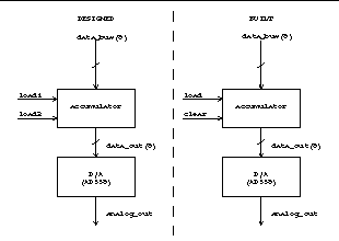
Original design
The original Accumulator design called for two independently loadable registers, whose output was averaged and sent to the D/A converter as shown in Figure 20. The original design was implemented in VHDL and synthesized on a Cypress 374I CPLD. The VHDL code is shown in Figure 21.
Accumulator VHDL(accumulator.vhd)
-- This is the accumulator code for the
-- Helium Breath Lab3. The output is the
-- arithmetic average of two values
-- each of which is stored by asserting the
-- load1 or the load2 signals.
data_bus : in std_logic_vector(7 downto 0);
data_out : out std_logic_vector(7 downto 0));
ATTRIBUTE pin_avoid of accumulator:entity is
-- these are all assuming the K1 kit connector is connected properly
-- " 1 2 11 21 22 32 42 43 44 53 63 64 74 83"& -- Vdd, Gnd, VPP
" 12 19 73 "& -- These pins are the interconnect bus
-- for CPLD 2, 3, and 4. They are Serial I/O
" 13 "& -- This is I0-9. Can screw up the clock of C1. Be
" 14 35 41 51 72 " & -- Used by Programmer. No external connection.
" 12 19 73 " & -- cpld interconnect bus
" 5 6 7 8 9 10 15 16 17 18 67 68 69 71 " & -- rest of the MCU data (L1-0
" 33 34 36 37 38 39 40 45 46 47 48 49 50 52 54 " & -- data to/from other cpld
" 75 76 77 78 79 80 81 82"; -- L2-0 through L2-7
attribute pin_numbers of accumulator:entity is
"load:3 clear:4 op_code:70 " &
"data_out(0):24 data_out(1):25 data_out(2):26 data_out(3):27 " &
"data_out(4):28 data_out(5):29 data_out(6):30 data_out(7):31 " &
"data_bus(0):55 data_bus(1):56 data_bus(2):57 data_bus(3):58 " &
"data_bus(4):59 data_bus(5):60 data_bus(6):61 data_bus(7):66";
architecture timingarch of accumulator is
-- result of adding the two data registers
signal internal_sum : std_logic_vector(8 downto 0);
-- the outputs are combinational
-- data out is the internal sum divided by 2
data_out <= internal_sum(8 downto 1); -- chop off the lsb to divide by two
process(clk, op_code, load, clear, data_bus)
if (op_code = `1') and (clear = `1') then
internal_sum <= (others => `0');
elsif (op_code = `1') and (load = `1') then
Implementation problems
Despite a large amount of time spent trying to get the Accumulator to work, its behavior never matched the specification given in by the VHDL code. The reason for the discrepancy between description and operation was never ascertained. The discrepancy was the source of much confusion and anguish in the debugging process.
Alternate design
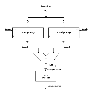
When it became clear that the original design could not be made to work, an alternate approach was undertaken. The alternate approach approximates the original accumulator design. The alternate Accumulator only has a single load signal which averages the current output with the current input to yield the new output. The output of the original design does not depend not on past signals as does the output of the alternate design, therefore the original design was a better. However, the approximate design could be implemented. The implemented Accumulator design is shown in Figure 22, and the VHDL code for the 22V10 8 bit register is shown in Figure 23.
VHDL code for 22V10 accumulator flip flop(8bitreg.vhd)
-- an 8 bit loadable, clearable register for a
-- 22V10. A 22V10 was used to make the wiring easier.
data_in : in std_logic_vector(7 downto 0);
data_out : out std_logic_vector(7 downto 0));
attribute pin_numbers of reg8:entity is
"data_in(0):4 data_in(1):5 data_in(2):6 data_in(3):7 " &
"data_in(4):8 data_in(5):9 data_in(6):10 data_in(7):11 " &
"data_out(0):23 data_out(1):22 data_out(2):21 data_out(3):20 " &
"data_out(4):19 data_out(5):18 data_out(6):17 data_out(7):16";
architecture timingarch of reg8 is
Timing
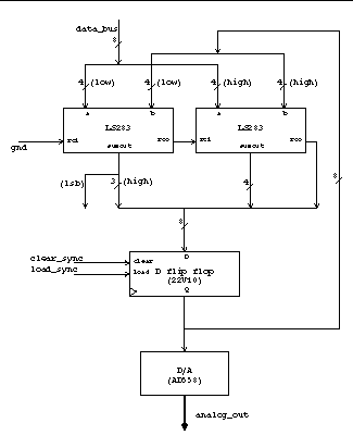
External Synchronization
The external control signals from the MCU to the RAM, to the Accumulator, and to the A/D were synchronized using the scheme shown in Figure 24. The assertion logic presented in Figure 24 does not assert the output signals if the opcode is 0 (jumps) and it holds the asserted signal for the whole of the following clock cycle
External synchronization circuit
The extra synchronization circuitry was necessary for two reasons. First, both the output from the program counters (74LS163, see Figure 10) and the output from the PROMs is glitchy. To avoid problems with glitches on the control signals, the PROMs are only enabled for the last half of the clock cycle. The rest of the pitch shifter only looks at the values of the control lines at the rising edge of the next clock cycle, so the synchronization circuitry holds the asserted signal for the next clock cycle.
The second reason that the circuitry in Figure 24 is necessary is that if the MCU is jumping to a new address, the address is contained in the same bits of the 16 bit instruction as the assert signals. The synchronization circuit forces the output signals to 0 if the opcode indicates that a jump is occurring (opcode = 0) by tieing the n_reset pit to the opcode.
6264 RAM timing
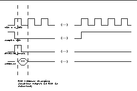
Although the 6264 RAM is advertised as a static RAM, if the address lines change while the RAM is active (CS1 high and n_CS2 low), the I/O pins suddenly drive the bus regardless of the state of the output enable (n_WE) signal. Originally unaware of this subtly, the design called for the RAM to always be enabled by wiring the CS1 pin high and the N_CS2 pin low. After observing unaccounted behavior from the RAM and re-reading the lab 2 handout, the n_CS2 pin was wired to the clock. The RAM therefore was active only for the last half of each clock cycle. Enabling the RAM on the last half of the clock cycle gave the address lines time to stabilize before enabling the RAM. Figure 25 shows the eventual RAM timing that was used.
Debugging Strategy and Experience
Implementing lab 3 involved two painful but separate experiences. Both experiences could have been significantly more painful had the design been more complex. In addition, debugging was aided by implementing the pitch shifter one module at a time. Each module was thoroughly tested before the next module was implemented. By building one module at a time, the possible source of errors were kept to a minimum.
MCU checkoff: make a detailed diagram
Provided with lab 3 was a simple MCU program and assertion logic which caused lights to blink in a particular order. This program was supplied to give an indication that the MCU was working properly before the other modules of the pitch shifter were implemented. Figure 26 shows the specification file for this test program. Figure 27 shows the assembly code for the test program, and Figure 28 shows the VHDL code for the assertion logic. All three files were provided by the 6.111 staff.
The MCU was built without the aid of detailed wiring diagrams with pin number. While the MCU eventually worked, several wiring mistakes were made that were hard to track down. When implementing the rest of the system, detailed diagrams were made before wiring. Because of these wiring diagrams (attached), very few wiring mistakes were made in the rest of the pitch shifter.
MCU test specification file (mcutest.sp)
/* assembler spec for debugging and testing of 163-based MCU */
/* (adapted from mcu.sp for AM29C10A-based MCU) */
/****************************************************************/
/* Instruction Word Organization: */
/* conditional branches 0cccxxxx aaaaaaaa */
/* unconditional branches 0111xxxx aaaaaaaa */
/* assertion statements 1sssssss ssssssss */
/* where c = status selection */
/* a = alternative address, i.e. jump address */
/****************************************************************/
op <15:0>; /* Indicates the available bits */
address op <7:0>; /* Indicates bit locations for addresses */
* There is nothing magic about upper case.
* You may change things to lower case as you wish.
* Remember, the assembler maps all characters to lower case anyway!
* Instruction set for your MCU
CJMP op<15>=%b0; /* Conditional JuMP */
JMP op<15:12>=%b0111; /* unconditional JuMP */
ASSERT op<15>=%b1; /* unconditional ASSERT */
/* These are defined so that you may use them to make your code more
* readable. Their use is not required. */
TRUE op<14:12>=%b111; /* This causes the 151 to output true */
RESET op<15:0>=%b0111000000000000;
* Status signals: Switches and frequency divider output OSC
* Make sure that all status signals that change during mcu operation
MCU test assembly code (mcutest.as)
/* assembler code for debugging and testing of 163-based MCU */
/* (inspired by mcu.as for AM29C10A-based MCU) */
# SPEC_FILE = mcutest.sp; /* This statement is required at the
beginning of the ASSEM_FILE. It tells
where the SPEC_FILE can be found. */
# LIST_FILE = mcutest.lst; /* This statement specifies the name for
the assembler listing file. If not
included, no listing will be created */
# MASK_COUNT = 8; /* This statement is required to mask out 8
bits of the 16 bit op-code to produce 2 PROM
files. Use with the `assem16to8' command. */
# SET_ADDRESS = 0; /* This statement tells the program at what
address to start assembling. The address
given is a hexadecimal number. */
# LOAD_ADDRESS = 100; /* This statement, if used AFTER the
SET_ADDRESS statement, determines the
beginning PROM address for the program
image. The address is in HEX. */
/* To execute this code, you should use the PAL file mcutest.pal.
*Beware!* The code has been placed in memory starting at HEX 100 so
you can use the same EPROMs for the debugging code as well as your
regular code. Wire address bit A8 of your EPROMs to +5 (or connect it
to one of your switches) to execute this code. Check the pal file,
mcutest.pal, and the specification file, mcutest.sp, to determine
wiring from the EPROMs to the PAL.
The OSC input to the multiplexer is reference frequency which tells
the LEDs how fast to blink. Any frequency within the range of about
10 to 20 Hz should work well. You should generate this frequency by
completing the mcutest.vhd file to create a counter which divides your
sampling clock by some appropriate amount. Then toggling the sampling
frequency selector switch will change the blink rate of the lights.
If nothing works, hook up your logic analyzer and follow the addresses
being executed. Use the mcu.lst file to follow the flow of
instructions and to see exactly what should be on the prom outputs and
the sequencer inputs. Check to see that the 163s are getting the
correct opcode at their LD inputs. If the opcode is a JMP, are the
163s getting the correct branch address at their ABCD inputs? Do they
load that address on the next rising edge? */
START: ASSERT CLRLEDS; /* Test to see if program counter increments*/
ASSERT; /* If PC does not increment, test to see */
JMP LOC4; /* that EnT and EnP of the 163s are wired high */
FAIL1: RESET; /* If code reaches here, then test your */
/* The following lines of code attempt to check each bit of the branch
address individually. As each bit is checked, we turn on the
corresponding LED. We try to branch to addresses 4, 8, 16, 32, 64,
and 128. Address 67 takes care of bits 0 and 1. The code at PROC1
doesn't get executed until after all these tests pass. */
/* The fun stuff begins here. */
/* When we get to this point for the first time after a reset, and all
switches are off, all 8 LEDs should be lighted. If not, we shouldn't
have gotten to this point anyway. But the problem probably lies in
the branch address wires from the EPROMs to the 163s. */
/* We wait here for a switch. */
BEGIN: CJMP S5 PROC2; /* If Switch 5 = 0 then execute PROC 1 */
JMP PROC1; /* Otherwise execute PROC 2 */
/* Proc two causes the LEDs to display a "roving eye". Switch 1
controls the right-moving half of the eye and switch 0 controls the
left-moving half. Switch 4 controls the speed. */
/* A right-moving roving eye */
/* A left-moving roving eye */
/* Proc 1 allows you to turn on and off leds 0 through 4 using the
PROC1: CJMP S0 LIGHT0; /* This checks LEDs 0 -> 4. Each LED can */
MCU test assertion logic (mcutest.vhd)
--------------------------------------------------------------
-- VHDL code for debugging and testing of 163-based MCU --
-- and getting your feet wet with a CPLD and the programmer --
-----------------------------------------------------------------
-- We have provided you with the headers and entity --
-- declaration for a counter. You should design this counter --
-- to take as input your sampling frequency signal and produce --
-- a signal in the range 10-20 Hz on the osc output. The --
-- osc signal is a conditon input to your MCU which controls --
-- the blink rate of the LEDs in the MCU checkoff. --
-- This is intended to be a fairly simple exercise in VHDL --
-- and should only require a few lines of code. Talk to a --
-- TA or a friend if you don't see how to do it. --
-----------------------------------------------------------------
port (sampclk : in std_logic; --This is the sampling clock
osc : out std_logic); --This is a 10-20 Hz signal
attribute pin_numbers of mcutest:entity is
architecture archmcutest of mcutest is
signal int_cnt : std_logic_vector(8 downto 0);
-- flip the values of internal oscillator when
-- we have counted all the way around
-- change osc when the output is all ones
end architecture archmcutest; --"architecture" is optional; for clarity
Accumulator: VHDL is not your friend
The VHDL code provided for the original Accumulator design is very simple and should have worked. Instead, it cost a day of debugging time to realize that it did not. It is suspected that the problem arose because the Accumulator and Storage Unit were placed on separate CPLDs and a signal conflict occurred. The suspicion has not been verified, and is suspect itself because The Storage Unit worked correctly. After checking all of the other modules comprising the pitch shifter, the Accumulator VHDL code was compiled with different options. The Accumulator still did not work as intended, but it behaved differently, leading to the conclusion that something was wrong in the process between the VHDL implementation and hardware implementation. After trying to make the CPLD do what was intended for half a day, the alternate (and less optimal) approach was adopted. The lesson learned from this debacle was that misbehaving CPLDs are very hard to debug because the internal signals are not visible, and hence can not help with debugging.
Conclusion
The pitch shifter is a very complex device. Even though thoughtful care was taken in the original design, problems inevitably arose. By keeping the device as simple as possible and still retaining the desired functionality, time was saved in the debugging process. The majority of the time spent implementing the pitch shifter was in the debugging process, an all too common occurrence. Detailed wiring diagrams cut down the debugging time as did careful wiring. It took a major effort to determine that the Accumulator was malfunctioning. Once the malfunction was isolated, however, only a few hours were necessary to create an alternate design and produce a working Accumulator. Overall, simplicity and a good debugging strategy are essential to the design and implementation of a complex system.