(VTTS)
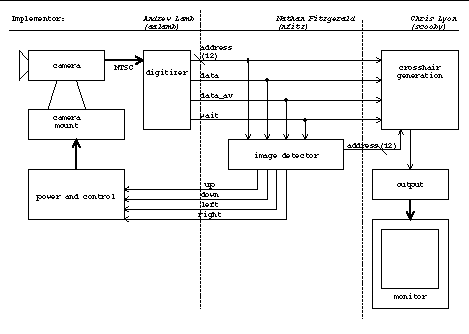
Nathan Fitzgerald, Christopher Lyon, Andrew Lamb
Table of Contents
Digitizer-Analog (Andrew Lamb) 4
Why NTSC is tricky to digitize 5
Digitizer-Digital (Andrew Lamb) 10
Target Detection (Nathan Fitzgerald) 20
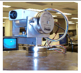
Camera Mount (Nathan Fitzgerald) 27
Video Output Unit (Chris Lyon) 27
Appendix A: Digitizer VHDL and MCU code 37
Appendix B: Monitor output VHDL and MCU code 52
List of Figures
System diagram of the Digitizer 4
Timing of digitizer data and control signals 5
Sync recovery and A2D wiring diagram 8
Schematic of an analog comparator with variable threshold 8
Oscilloscope trace of NTSC signal, HSync, and color burst 9
Oscilloscope trace of NTSC signal and Even 9
Oscilloscope trace of NTSC signal and discriminator output 10
Oscilloscope trace of NTSC signal and vertical blanking 10
Address and buffer unit block diagram 11
Oscilloscope trace of inter-kit communication lines 14
Oscilloscope trace showing clk and fastclk 15
Block diagram of the hskip module 16
Address and buffer unit counters 16
Detector refined block diagram 21
Stepper motor system diagram 24
Stepper motor coil configuration 25
Stepper motor FSM block diagram 25
Stepper motor wiring diagram 26
Video Output Unit Block Diagram 27
Storage Unit Circuit Diagram 28
Memory Storage Timing Diagram 29
Modification Unit Circuit Diagram 31
Memory Modification Timing Diagram 32
Memory Copy Circuit Diagram 32
Introduction
VTTS in the Real World
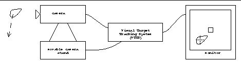
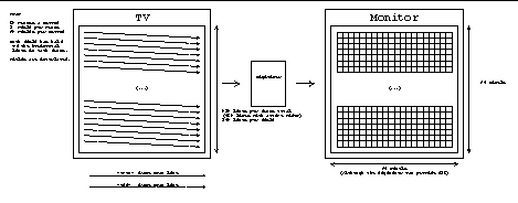
The Visual Target Tracking System (VTTS) is a system for visually tracking targets using a gimbal mounted camera and digital control circuitry. A small black and white camera is mounted on a stand that can be moved with two directions of freedom. When an object is placed in the camera's field of view, the camera moves such that the object becomes centered in the camera's field of view. The camera's progress is monitored by a Television monitor which will display both a center square and a crosshair overlay on the center of the object. Figure 1 shows how the VTTS is connected to the real world.
Digitizer-Analog (Andrew Lamb)
System diagram of the Digitizer
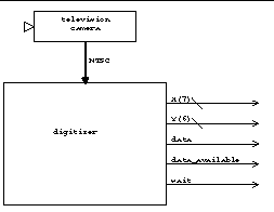
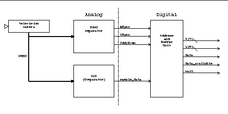
The digitizer takes an NTSC video signal from a standard video camera and presents a 64x64 pixel grid of black and white pixels for output and image detection. The digitizer outputs a 7 bit X address, a 6 bit Y address line, a data line and communication signals data_available and wait. Figure 3 shows a system diagram of the digitizer.
The astute reader will realize that to address a 64x64 grid only 6 X address bits are required. The original design called for 192x128 (8 bits X, 7 bits Y) resolution, but as details about implementation became clearer the resolution was dropped to 64x64, yet the digitizer's design is capable of capturing the full 192x128 pixels. Unfortunately, much of the digitizer's complexity is due to the fact that it is capable of capturing in 192x128 mode, even when a lower resolution was finally used in the project. Internally, the digitizer still creates a 128x64 pixel grid, and the low X address bit is ignored by the other modules.
Timing of digitizer data and control signals
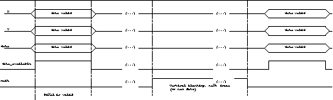
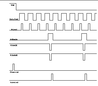
The digitizer generates two communication signals in addition to the pixel address and data. The wait signal is high while the digitizer is buffering the next NTSC frame from the camera. When the wait signal is high, the other kits can perform the computation necessary for image detection and crosshair overlay. When the wait signal goes low, new data and address information is sent. To signal that the data and address lines contain valid information, the data_available signal is brought high. The digitizer keeps the address and data lines stable while data_available is high. Figure 4 shows a timing diagram for inter-kit communication.
Why NTSC is tricky to digitize
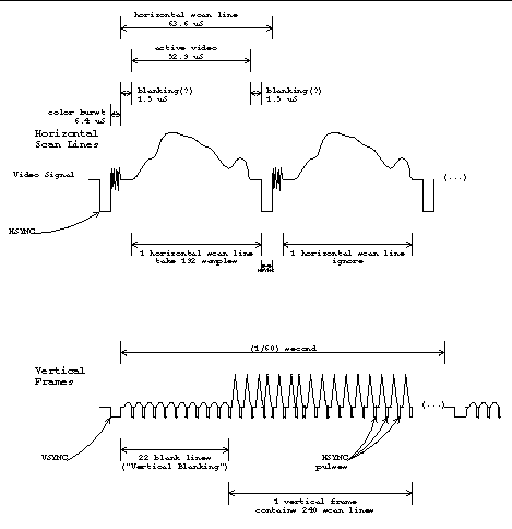
The standard for broadcasting TV signals in the United States is called NTSC (National Television Systems Committee). NTSC was first proposed in 1940 and was standardized in 1953. Televisions sweep an electron beam horizontally across a phosphor coated screen, starting from the upper left and working downward. The phosphors emit light when struck by the electrons, and by changing the strength of the electron beam, the phosphors that are excited change and create a moving image.
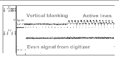
There are 525 horizontal scan lines in each NTSC frame (a frame is one complete screen). Each NTSC frame is divided into 2 fields of 262.5 horizontal lines each. The first field contains the even horizontal lines, and the next field contains the odd lines. Even and odd fields are interlaced between each other. Figure 5 shows the relationship between the even and odd horizontal lines in each field, and the format of the digitizer's output. 30 frames (or 60 fields) are sent each second, and the first 22 horizontal lines in each frame are blank (called vertical blanking) to allow time for the electron beam to return to the upper left corner of the screen. The useful part of NTSC (with active video information) is 480 horizontal lines (240 per frame) of continuos voltage levels.
Using only a single wire and 6 MHz of bandwidth, all of the information for both colors and electron bean movement are somehow transmitted in an NTSC signal. The end of each horizontal line is marked by a horizontal sync pulse of -1 Volt. The end of a frame is marked by another, longer pulse of -1 Volt called the vertical sync.1
NTSC conversion
The digitizer converts the NTSC signal into a 64x64 grid of black and white pixels. The timing of the NTSC signal is crucial for the digitizer to work correctly, so NTSC timing is described in gory detail below.
A schematic view of the NTSC signal is shown in Figure 6. After the end of a horizontal sync, there is 7 uS "back porch" before active video data is available. In the 1957 revision of NTSC to support color, the "back porch" contains a "color burst" (see Figure 9 for an oscilloscope trace of an actual color burst) that sets the palette of colors that will be used for the upcoming data. The "color burst" is used to synchronize a phase locked loop, whose output is used to separate out chrominance and luminance information from the active video by some magical process. Color is way beyond the scope of the VTTS, and therefore the digitizer is interested only in the intensity of the signal so all color information is discarded. To avoid digitizing the back porch and colorburst, the first 7 uS of each horizontal scan line are ignored. After the first 7 uS there is active video for 51.8 uS in the form of a continuos voltage level.
Sync recovery
NTSC is a very analog format, and the VTTS dreams in digital. The digitizer must therefore convert all of the NTSC analog tom-foolery into clean digital signals. A GS4981 sync recovery chip was used to detect the horizontal and vertical sync pulses, and an LM311 was used as a comparator to compare the NTSC data voltage to a predetermined threshold.
Sync recovery and A2D wiring diagram
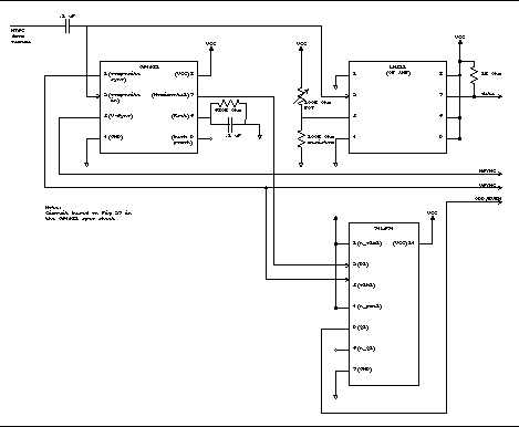
The GS4981, while obsolete, works well when it is configured properly. Unfortunately, the application notes presented in the GS4981 spec sheet were hard to understand. There were about 5 test circuits which did not work. By trial, error and some luck, the circuit in Figure 7 was arrived at. This circuit gives a negative true HSYNC signal that is low during a horizontal sync and high otherwise. The circuit also gives a negative true VSYNC which is low during a vertical sync and high otherwise. Another useful signal derived from the VSYNC signal is the EVEN signal that is true for alternate frames, and provides a measure of relative location within a frame. The EVEN signal can be used to detect the start of individual frames.
Discriminator
The digitizer converts the continuous analog voltage level of the NTSC signal into a logical one or a zero. To perform the conversion, an analog comparator with a variable reference voltage was used2. Figure 8 shows a schematic for the discriminator circuit that was constructed. The reference voltage is set by placing a potentiometer in a voltage divider. By changing the resistance of the potentiometer, the threshold voltage can be either raised or lowered. The potentiometer is lovingly called the discriminator, and it functions like the contrast dial on a television set, allowing the VTTS to discriminate objects from the background.
Implementation
The wiring of both the sync recovery circuitry and the discriminator is shown in Figure 7.
Although schematics of the NTSC signal were provided during the design phase, many subtleties such as the vertical blanking, back porch and color burst were only apparent after the initial implementation. Therefore, included for the reader are actual oscilloscope traces of an NTSC signal and the corresponding output from the sync recovery circuitry and the discriminator in Figures 9, 10, 11 and 12.
Digitizer-Digital (Andrew Lamb)
Digitizer block diagram
While the analog parts of the digitizer are interesting, the major functionality (and therefore complexity) is in the address and buffer unit. Originally, the digitizer was conceived of as some combinational logic with some counters that generated addresses with the hsync and vsync digital signals. Unfortunately, the original system design also called for 192 samples per horizontal line. To achieve a sample rate of 192 samples per line, an MCU buffering scheme was designed. Squeezing 192 samples per horizontal line determined much of the design for the digitizer, and by the time that the resolution was dropped to 64 samples per line, the digitizer design was already finalized and partially implemented.
Since 192 samples were to be taken over a period of about 50 uS, a minimum clock rate of 4 MHz would have been necessary. The 4 MHz number assumes a single sample can be processed each MCU cycle during a horizontal scan line, so 8MHz seemed a more reasonable estimate of the requisite clock speed. However, since the 6.111 "nerd kit" has a top safe speed of around 10MHz, 8MHz seemed too close to pushing the limit. Somehow the other kits would have had to process data at least this fast, and quickly it became apparent that an alternate approach was necessary.
Since only 64 of 262.5 possible horizontal lines are digitized, much of the NTSC data is ignored, and the digitizer spends a lot of time waiting for new data to sample. By buffering data into a RAM during one frame, and then playing it back out slowly and evenly during the next frame, the other kits have the necessary time to process the incoming data.
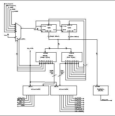
A buffering unit was implemented that is capable of storing a screen's worth of data and then slowly playing the buffered data back out to the other units. Figure 13 shows a block diagram of the entire digitizer module.
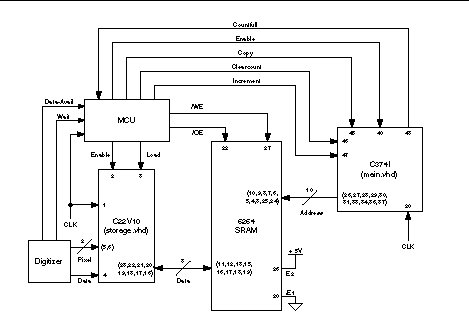
Address and buffer unit block diagram
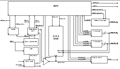
The address and buffer unit does nothing more than buffer a screen's worth of data and then play it back slowly. Unfortunately, it requires a RAM, an MCU, various counters to address the RAM and clock trickery to sample data quickly. Figure 14 shows a block diagram of the address and buffer unit.
The address and buffer unit actually takes 128 samples per line, even though the resolution used by the other kits is 64 horizontal samples. By the time that it was decided to drop to 64 pixels, the address and buffer unit had already largely been constructed, and it was easier to ignore the lowest X address bit than to redesign the digitizer.
Sampling strategy
To take 128 evenly spaced samples over 50 uS of active data with a 1.75 MHz system clock, at least 2 samples per MCU cycle must be taken. The overhead of driving a bus, incrementing counters, writing to the RAM, and looping dictates 3 MCU instructions. The addressing and storage unit must therefore be able to capture 8 bits of data in 4 MCU instructions. By using a fast shift buffer, the 8 previous bits of data are latched at once from the fast shift buffer, and written to a single location in RAM while the next 8 data bits are being stored in the fast shift buffer. Then the next 8 bits are latched, and the process repeats until the end of the horizontal line.
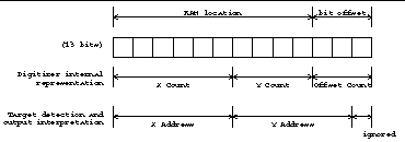
The fast shift register in the address and buffer unit is called the fast sample unit. The fast sample unit is the only module in the address and buffer unit that is clocked with the 3.5 MHZ clock. The 6264 RAM used in lab 3 has 8 data bits per address location, so all 8 samples can be stored in one memory location. The upper 6 bits of the RAM address are the current Y location (current line). The lower 4 bits of the RAM address are the upper 4 bits of the X address. Within each RAM data byte, the most significant bit is the first bit that was sampled. Therefore, the lowest three bits of the X address are the data bit's offset within the byte. Figure 15 shows how an pixel address relates to its storage location in RAM.
Pixel addresses
The 4 instruction algorithm to sample a single horizontal line is as follows. (Note: the rising edge of HSync can be used to determine when a particular horizontal scan line starts):
Example storage locations
Figure 16 is an example of the fast sampling strategy. The pixels at (64,32) through (71,32) will be stored into the same location in RAM. The RAM address is computed by taking the Y address and concatenating it with the high 4 bits of the X address. The low three bits of the X address are referred to as the Offset, and they denote at which location in the byte that particular bit of data is stored.
Playback strategy
To transmit data to the other kits, one bit of data and a 12 bit address are sent, along with the data_available and wait signals. Since the address and buffer unit stores 8 bits of sampled data in the same memory location, the entire 8 bits need to be read out and the appropriate offsets communicated to the other kits. The output unit loads data from a RAM location, and then shifts out the bits one by one to the other kits, incrementing an offset counter each shift.
The algorithm for sending a buffered byte of data:
- Select the top 10 address bits (Y Counter and X Counter).
- Read the data byte stored at that location into the output unit. The output unit will show the data at offset 0 and the Offset Counter will be at 000.
- Set data_available line high for long enough for the other kits to process the current data bit.
- Increment the Offset counter and shift the output unit to the next bit. The output unit will now show the data at offset 1 and the Offset Counter will be at 001.
- Repeat for each of the 8 offsets.
- Select the next top 10 address bits, load the next byte, and repeat until the entire buffer has been transmitted.
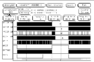
Figure 17 shows an analyzer trace of the communication lines between kits.
Clock generation
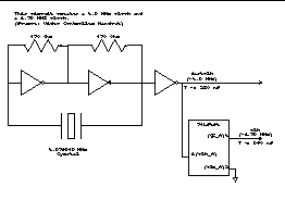
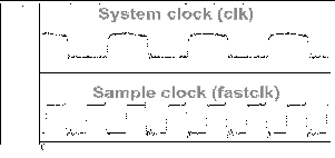
For the address and buffering unit, a fast clock and a slow clock derived from it are necessary. The circuit for a 3.5 MHz clock from the video controller handout was used as a starting point for clock generation.The sampling clock is a 3.5 MHZ signal with a measured period of 280 nS. The system clock is the sampling clock divided by a factor of two to 1.75 MHZ with a measured period of 560 nS. A circuit diagram for the clock generation is shown in Figure 18, and Figure 19 contains an oscilloscope trace which illustrates their relationship.
Fast Sample block diagram
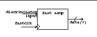
The fast sample unit shown in Figure 20 is a shift register that saves the value of the discriminator output for the last 8 fast clock cycles. Every 4 system clock cycles 8 data points have been stored, with the more recent data value being in the least significant bit position. Appendix A contains the VHDL code for the fast sampling unit.
Synchronizer block diagram
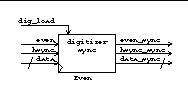
Since the fast sampling unit runs on a different clock than the rest of the system, its outputs must be treated asynchronously. The digitizer synchronizer is used to latch the current 8 data bits from the fast sampling unit when the dig_load signal is asserted. By latching the 8 bits from the fast sample unit using the synchronizer code in Listing 4, the last 8 data bits can be held stable enough to write to RAM. Since the RAM must also be able to write to the bus, the output from the digitizer synchronizer is tristated using another PAL as an 8 bit tristate buffer.
The digitizer synchronizer also synchronizes the hsync and even signals from the sync recovery circuitry to the system clock in the same PAL to reduce the number of chips necessary. All of the VHDL code for the synchronizer and the tristate buffers can be found in Appendix A.
Block diagram of the hskip module
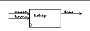
Figure 22 shows a block diagram of the HSkip module. The HSkip module is a resettable counter that counts hsync pulses and asserts the done signal when 16 horizontal sync pulses have passed. The HSkip module is reset at the beginning of each field, and by counting 16 horizontal lines, the vertical blanking period is skipped digitized. The initial version of the digitizer had 16 blank lines at the top of the screen because it was sampling during the vertical blanking period. The code for the HSkip module can be found in Appendix A.
Address and buffer unit counters
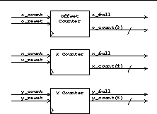
Figure 23 shows the three counters that the address and buffer unit uses. The O Counter is the 3 bit counter used to select the data offset within a byte, the X Counter is the top 4 bits of the X address, and the Y Counter is the entire Y address. All of the counters are resettable and only count on clock cycles that their count signals are enabled. When the counters have reached their maximum counts (23 for O Count, 24 for X Count, and 26 for Y Count) they assert a full signal which is available to the MCU. The X counter is wired to the low four bits of the RAM address and the Y counter is wired to the next six bits of the RAM address. The VHDL code to implement the three counters is in Appendix A.
Output unit block diagram
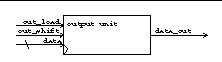
The output unit is a loadable shift register. When the out_load signal is asserted, the 8 bit value on the data bus is latched by the output unit, and the highest bit is passed on to data_out. When the out_shift signal is asserted, the internal register is shifted to the left by one, so the next highest bit is now passed on to data_out. The output unit is used to unpack data bits that were packed by the fast capture unit one at a time. The MCU controls playback by loading a byte from RAM into the output unit, and then shifting the data back out one bit at a time. Since the MCU controls playback, inter-kit communication timing can be changed by updating MCU code. Appendix A shows the VHDL code for the output unit.
Ram Wiring
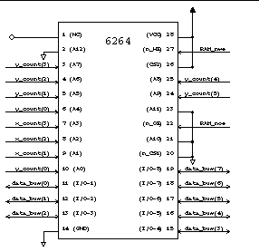
A standard 6264 Random Access memory (RAM) was used to buffer each byte of data. Figure 25 shows the wiring scheme that was used.
MCU block diagram
The Microcontroller Unit (MCU) that is used for the address and buffer unit is the same MCU that was used for lab 3. The MCU from lab three has two types of instructions, an ASSERT and a CJMP (Conditional JumP). An ASSERT instruction's highest bit is a 1 and a conditional jump's highest bit is a 0. Figure 27 shows the MCU instruction format.
MCU instruction format
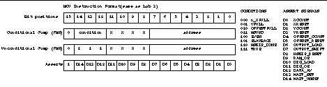
A clever reader will realize that the MCU can not assert a RAM write pulse. Instead of expanding the MCU's data word (which would have involved adding an additional prom to the MCU) a "clever" hack was introduced. A PAL is connected to the address lines of the MCU and it asserts the negative true write pulse for the RAM whenever a particular instruction was executed. Figure 28 shows a block diagram of the MCU. Appendix A shows the VHDL code for the RAM write hack. Tables 1 and 2 summarize the MCU input and output signals.
Appendix A contains the MCU assertion logic. Somewhat interesting is the fact that the wait signal is settable/resettable by the MCU. When the MCU asserts a WAIT_SET signal, the wait signal is set to high, and the wait signal remains high until the MCU asserts a WAIT_UNSET signal which causes the wait signal to go low.
The MCU code presented in Appendix A implements the sampling and playback algorithms presented in the sampling strategy and playback strategy sections above. The MCU assembler listing in Listing 24 is included to show where the RAM write occurs. The ramwrite.vhd code states that when address 1C is being executed the RAM write pulse is asserted low. Since the assertion logic latches the PROM values the cycle after the address has been asserted, the write pulse actually happens the same clock cycle as the assert signals at MCU address 0x1B.
Target Detection (Nathan Fitzgerald)
Detector block diagram
The goal of the target detector system is to determine the location of the target from the video data given by the digitizer. It then outputs the x-y coordinates of the target to the video output unit for crosshair overlay and outputs a directional signal (up, down, left or right) to the camera control unit. A high level block diagram of the detector appears in Figure 28. The design fits almost entirely on three Cypress 374I CPLDs (Complex Programmable Logic Device). Only 3 external PALs (Programmable Array Logic) are required. This means that the design could be transferred between 6.111 kits with relative ease, limiting the number of inter-kit transmission lines.
The detector works by finding the "center of mass" of all white pixels on the screen, and assuming that the center of mass is the center of the target. The unit operates in two modes. In the first mode, the x and y addresses of all white pixels are summed separately and the total number of white pixels on the screen are counted. No memory is required for this function; the data is summed sequentially as it is received from the digitizer. In the second mode, the x and y address sums are divided by the total number of pixels to determine the average address.
The division step required the most engineering of all the parts that make up the detector. The limiting factor is the size of the x and y address sums and the white pixel counter. If the target occupies the entirety of the screen, all the pixels will be white. On a 64 x 64 screen, that means that the white pixel counter has to be able to reach a value of 4096, which is a 12 bit number. The x and y address sums must be able to reach a value of 258,048, an 18 bit number. The number of flip-flops required to implement the counters and shift registers necessary to do the calculation is quite large and is difficult to fit on a single Cypress 374I CPLD. The solution to this issue is to break the calculation between multiple CPLDs, however the number of pins on the CPLD board then becomes the limiting factor. Sending 19-bit buses between CPLDs quickly uses up the limited number of output pins on the CPLD board. The detector design is elegant because it makes use of multiple CPLDs on the CPLD board and limits the number of output pins and inter-CPLD connections required.
Detector refined block diagram
A refined block diagram of the design appears in Figure 29. Two CPLDs are dedicated to the averaging calculations of the x and y addresses. They input the address given by the digitizer as well as control signals from a finite state machine (FSM) that controls what address is assumed to have a valid white pixel and also control the mode of calculation (summing vs. division). During the division mode, these units serially output the average address to two 22V10 PALs, which act as shift registers that deserialize the target address. The FSM controls when the PALs stop shifting in serialized data. A motor control PAL (a 20V8) compares the x and y target addresses to the address of the center of the screen to determine the direction that the camera must pivot in order to move the target to the center of the screen. The source code for the CPLDs appears in Appendix B.
Detector FSM
The states of the FSM appear in Figure 30. Only three states are required to control the detector. In the reset state, a restart signal is asserted that clears the counters in the x and y detectors. The mode of the detectors is set to 0 (adding mode) and the system stays in that state until the wait/end-of-frame signals go low and the detector begins giving valid data. Then the FSM moves to a load state where it screens the data signal from the detectors for valid data, i.e. data that is high while data_available is high, and passes valid signals on to the detectors. The FSM remains in this state until the end of the frame. Then the FSM transitions to an averaging state, and the mode output changes to 1 (divide mode). A counter internal to the FSM begins counting the number of clock cycles that the FSM has been in the Average mode. During this time, the detectors are serially transmitting data to the deserializers. After 7 clock cycles, the FSM signals the deserializers to stop collecting data and output the target addresses. The FSM then resets itself and begins waiting for new data.
Detector Divider
The division works by implementing an algorithm similar to the one taught to elementary school students by using a shift register, comparator, and subtractor. A diagram of this unit appears in Figure 31. The algorithm differs from the one taught to elementary school children in that it makes use of the fact that it being used to find an average. It is known that the quotient will be a 6 bit number. It can therefore be assumed that the denominator is greater than the first 12 bits, and so the standard division algorithm can begin at the 13th bit. This cuts down the size of the shift register needed to do the division, making it easier to fit on the CPLD.
The deserializers are essentially shift registers that are enabled by a signal from the FSM. They do, however, have one additional feature. It is known that the quotient is a 6 bit number, but the system is designed to handle 7 bit division. In the event of a blank screen, a divide-by-zero will occur, and the detectors will output a stream of ones to the deserializers. Having the extra bit allows the deserializer to distinguish between a blank screen and a target located at x = 31 and y = 31. In the event of a blank screen, the deserializers output the address of the middle of the screen. The deserializers were implemented in VHDL using 22v10 PALs. The source code appears in Appendix B.
The final part of the detector unit is the camera control unit. It basically compares the x and y target coordinates to the coordinate at the center of the screen. If the target is more than a few pixels away from the center, the appropriate up, down, left or right signal will be asserted to move the target to the center of the screen. The deserializers were implemented in VHDL using 20V8 PALs. The source code appears in Appendix B.
Camera Control
Stepper motor system diagram
After the target detection module determines the center of the screen from the digitized camera signal, the signals up, down, left and right are generated. These signals are used by the stepper motor electronics which control the actual motors which move the camera mount.
Electronics (Andrew Lamb)
A stepper motor is like a normal DC motor, except each of a stepper motor's coils can be controlled individually. Electric motors move because of magnetic repulsion between a permanent magnet and an electromagnet made by running current through one of the motor's coils. The motor rotates when the coils that current flows through are cycled through in a particular order. In a normal DC motor, mechanical motor brushes cause the correct coil activation sequence. In stepper motors, since each coil can be activated individually, the motor rotates a specific amount on each step. The stepper motors were configured as suggested by the 6.111 handout. Figure 33 shows a schematic diagram of the bifiliar configuration that was used. The motor coils are attached to the control lines IA+, IA-, IB+ and IB- to allow low current digital logic signals from PALs to control the high current stepper motors.
Stepper motor coil configuration
The stepper motors should not be powered from the 6.111 kit. The 6.111 kit, while having an 8 Amp power supply, is not set up to handle the surges that a stepper motor can generate, so an external power supply is used. The external power supply is controlled by the IA+, IA-, IB+ and IB- signals. When one of the IA+, IA-, IB+ or IB- signals is a logical high, a path is created from the external power supply to ground through the appropriate coil causing the stepper motor to advance to the next position.
To activate the coils in the correct sequence, an FSM is used to generate IA+, IA-, IB+ and IB- signals based on forward and reverse input signals. Originally, a four full-step sequence was implemented, but each step was too large when the mount was build. To decrease the step size, an 8 half-step sequence was implemented. Figure 34 shows the block diagram for the motor control circuitry, Table 3 shows the FSM states, and Listing 1 shows the VHDL code to implement the FSM.
Video Output Unit (Chris Lyon)
Overview
Once the video input signal from the camera has been captured, it is desired to overlay images of a square and a crosshair over it before outputting it to the TV Monitor.
Video Output Unit Block Diagram
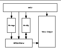
The overall system design is built around an MCU. A comprehensive block diagram can be seen in Figure 37. The Storage block is responsible for taking the signal from the digitizer, converting it to the appropriate format, and storing it in the SRAM buffer. The Modify block takes the original image, and overlays the images of the box and crosshair over it. Once the frame has been fully processed, it is passed to the Video Output block for display on a TV monitor.
Storage
In the graphics display mode used, each pixel can be displayed in one of four colors, at a resolution of 64 x 64 pixels. To allow for the color depth, each pixel must be represented by two bits in memory. Because of this fact, a single byte contains the color information for four pixels on the screen. To ensure that the digitized image is properly displayed in the end, this bit-packing scheme must be strictly adhered to. Unfortunately, doing so leads to a more complex data storage and modification scheme.
The digitized video signal is received from the Digitizer Unit one pixel at a time. Since four pixels must be stored in each byte, a PAL is used to build each byte. Once a byte has been completely assembled, it is written to the current location in memory. A circuit diagram for the Storage Unit is shown in Figure 38. The VHDL code for the Storage PAL is in Appendix C.
Storage Unit Circuit Diagram
A main counter programmed into a CPLD is used to increment the address lines to the SRAM. When the Digitizer is ready to send data, its WAIT status signal goes low. CLEARCOUNT is asserted to reset the address lines to the SRAM. Immediately following that, DATAAVAIL will go high, signifying that the first pixel's value is stable on the DATA line. The low two x address bits from the Digitizer are used to index the current pixel storage location within the byte being stored. As each pixel becomes available, SLOAD is asserted to read the current DATA value into the Storage PAL in the proper location. Once four pixels have been stored, the output of the Storage PAL is enabled, driving the new byte to the data bus. The memory write-pulse is then asserted, to write the byte to the correct location in memory. The main address counter is now incremented, and this process continues until the main counter sets the MCU status signal COUNTFULL. A timing diagram for the storage process is shown in Figure 39. The VHDL code for the Main CPLD is in Appendix C.
Memory Storage Timing Diagram
It is important to note that a slight modification has been made to the standard bit-packing convention for the video signal. The order of each byte has been reversed in memory, to simplify the pixel storage process pertaining to the two address lines. This modification is compensated for by swapping the order of the data lines at a later time when the contents of the SRAM is actually copied into the VRAM.
Modification Algorithm
Unfortunately, gaining the ability to perform a fully transparent overlay over the stored video image proved to be a fairly daunting task. To accomplish the overlay, it was necessary to have the capability of changing the color of one pixel at a time. Since four pixels are stored in each byte, the target byte must be read out, modified, and written back into the same location in memory. At the lowest level, this procedure is accomplished by performing an `AND' operation between the original byte and a masking field, after which the result is `OR'd with the new pixel's color value in the desired location. The overall modification algorithm is detailed in Figure 40.
Overlay Image Pixel Maps
Once the single-pixel-replacement strategy is possible, entire images can be copied over the captured video sequence one pixel at a time. The box and crosshair images are both stored in a PROM chip. The actual pixel maps for both images are shown in Figure 41, and the data file for the PROM contents can be found in Appendix C.
The images are actually stored as a sequence of x and y values for each pixel whose color is to be changed. Since both images are less than 16 pixels square, both the X and Y values can be stored in a single byte, with four bits allotted for each dimension.
As the images are stored, they are located in the upper left corner of the screen. During the process of copying them into main memory, offset values are computed and then added to the pixel locations being read out to locate the images at the desired screen locations.
Since the box is always located at the center of the screen, the location of each pixel being read out of the PROM just needs to have a constant value added to both dimensions. Once this value is computed, the result is directly outputted to the memory address and pixel select lines.
Performing the crosshair overlay is slightly more complicated. In this case, the screen offset for the image is received from the Detector. The data from the Detector must be latched to ensure that it remains constant throughout the entire operation. This latching is accomplished using two PALs. The VHDL code for these PALs is located in Appendix C.
Since the crosshair should always be completely on the screen, the offset value is overridden if it is too close to any of the edges. If the detected image lies near an edge, the crosshair will just appear at that edge. This manual offset override is handled by the CPLD. As before, the computed location for each pixel is output to the address and pixel offset lines.
A circuit diagram for the modification logic is shown in Figure 42. As the main counter increments the address lines to the PROM, the resulting pixel locations are returned and the offset is computed. The pixel locations are computed as 12 bit numbers, with the first six bits corresponding to the Y-location on the screen, and the last six bits corresponding to the X-location. The lowest two bits of the X-location are used as the pixel index within a byte, while the remaining high ten bits of the entire address are used to index the desired byte in memory. It should be noted that the SYMBOL assertion signal is used as the ninth address bit to the PROM, and determines which image is actually being read out by the 8-bit counter.
Modification Unit Circuit Diagram
To perform the actual memory modification, CLEARCOUNT is first asserted to reset the main counter. With the appropriate symbol selected by the MCU, the location of the first pixel is read out of the PROM and the offset is computed. Once the output address lines are stable, the target byte is read out by asserting RAMOE. That byte is then latched into the Modify PAL by asserting the MODLOAD signal. Once the pixel replacement algorithm is performed, the PAL drives the newly modified byte back onto the databus upon assertion of MODENABLE. Once the new data is stable, a memory write pulse is asserted to store the new byte in its previous location in the SRAM. The main counter is now incremented to handle the next pixel being replaced. This process continues until the SYMBOLDONE status signal is asserted by the CPLD. Since each of the two overlay images has a different number of pixels, the maximum value of the counter is dependent on which symbol is being read. A timing diagram of the modification process can be found in Figure 43. The VHDL code for the Modify PAL is in Appendix C.
Memory Copy Circuit Diagram
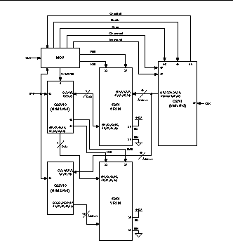
Once both images have been overlaid on the digitized video signal, the completed frame is ready to be output to the TV. Since the Video Output Unit is reading the screen data out of its own VRAM chip, the entire contents of the SRAM must be copied into the VRAM in order to be displayed. This process is complicated by the fact that the actual Video Controller must have unrestricted read access to the VRAM for almost the entire frame period.
During the vertical blanking period, the Video Controller relinquishes its access to the VRAM, and the contents can be rewritten. Since the blanking period only lasts for 2 ms, this operation must be accomplished quickly. Essentially, the address and data lines for both RAM chips are tied together. Upon inspection of the circuit diagram in Figure 44, the reader will notice that two PALs actually handle tristate buffering of the data, address, and control signals to the VRAM. This additional logic is necessary to prevent tristate bus contention, which could permanently damage the parts and cause erratic behavior. The VHDL code for the VRAM Tristate PALs is in Appendix C.
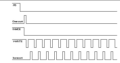
To begin the copy process, the address counter is reset to zero by asserting CLEARCOUNT. Since timing is of the essence due to the vertical blanking constraint, RAMOE will be held low for the entire copy process. With the main counter now addressing both RAM chips, and the data busses of both chips connected, the VRAM is seeing the data at the current location in the SRAM. A write pulse is asserted via the VWRITE signal to store the current byte in the VRAM. INCREMENT is now asserted to increment the main counter to address the next byte in both RAM chips. The VWRITE signal is again asserted to store the byte. This process is repeated until COUNTFULL goes high, signifying that the end of the used memory has been reached. Once every byte is copied and the vertical blanking period ends, control of the VRAM is returned to the Video Controller. A timing diagram of this process is shown in Figure 45.
Video Controller
The Video Controller is responsible for converting the digital composite video signal into the analog signals necessary to drive a TV Monitor. An MC6847 Video Controller chip is used to generate the synchronization, chroma, and luminance signals for the output. The MC6847 operates in mode CG1, providing for a resolution of 64 by 64 pixels with four possible colors per pixel. This operational mode is set by selecting the appropriate values for the 8 mode-select inputs to the chip. The output signals from the MC6847 are converted to RGB signals by combinational logic programmed into a PAL. The monitor receives the R, G, and B data lines, as well as the HSYNC and VSYNC signals. A full circuit diagram for the Video Controller Unit is shown in Figure 46.
Video Controller Unit Circuit Diagram
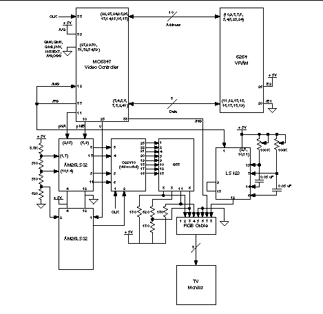
The MC6847 has unrestricted access to the VRAM chip, with its address and data lines directly connected. The HSYNC signal to the monitor is pulled directly from the chip with no modifications. The /FS signal from the chip however, must be passed through a one-shot timer to create the necessary delayed vertical synchronization pulse that is connected to the VSYNC input on the TV. /FS is also tied directly to the /MS input on the MC6847. This connection forces the MC6847 to relinquish control of its data and address lines during the vertical blanking period.
To create a color display, the Y, phiA, and phiB outputs of the MC6847 must be converted to Red, Green, and Blue values for the actual TV to display. These outputs must first be compared to predetermined voltages via AM26LS32 comparators to create a series of digital outputs. These digital outputs must then be passed through combinational logic to convert them to R, G and B values. The logic for this operation is programmed into a PAL. The VHDL code for the Video PAL is in Appendix C.
The final stage of combinational logic is implemented with S38 NAND gates. Since these gates are open-collector, they must be tied high with the specified resistor values. Using the S38 gates is what enables the Video Controller to produce the color Orange. Although Orange is not used in this specific project, it was desired to retain the ability to do so should the need arise. The Red, Green, and Blue outputs from the combinational logic are directly connected to the TV monitor.
MCU
The MCU used to drive the control signals for the entire Video Output Unit is identical in structure and function to that used in the Digitizer. The only difference lies in the assertion and condition signals. Table 4 details the purpose of the assertion signals used by the MCU. Table 5 explains the uses of the condition signals that govern conditional jump instructions in the main program. The MCU assembly and specification files, as well as the VHDL for the PALs handling the assertion logic are in Appendix C.
|
Low when the vertical blanking period for the Video Controller is occurring. |
||
Clock Distribution
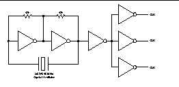
It is also important to note that a successful clock distribution scheme is essential to the proper functionality of the Video Output Unit. With many gates requiring clock signals, fan-out rules must be strictly obeyed. The entire unit is driven off of the 3.579545 MHz crystal oscillator required by the Video Controller. The circuit used for clock distribution is shown in Figure 47. No more than three clock signals should be connected to any of the three Inverter outputs.
Appendix A: Digitizer VHDL and MCU code
Stepper motor FSM (stepperhalf.fsm)
-- Stepper motor FSM for target tracking system
aplus, aminus : out std_logic;
bplus, bminus : out std_logic);
attribute pin_numbers of stepperhalffsm:entity is
architecture state_machine of stepperhalffsm is
type StateType is (s1, s2, s3, s4, s5, s6, s7, s8);
attribute enum_encoding of StateType:
type is "000 001 010 011 100 101 110 111";
-- the four states form a loop. Fwd asserted makes them
-- go in one direction, and rev makes them go in another
state_transition:process(clk,fwd,rev,reset,p_s)
begin -- change to the next state
-- outputs are only combinational
aplus <= `1' when ((p_s = s1) or
aminus <= `1' when ((p_s = s5) or
bplus <= `1' when ((p_s = s7) or
bminus <= `1' when ((p_s = s3) or
end architecture state_machine; --"architecture" is optional; for clarity
Vertical blanking skipping VHDL for HSkip (hskip.vhd)
-- resetable timer that counts 16 hsync
-- pulses and then asserts a blank_done signal
-- this is necessary becuase there are blank lines at the top
-- of a NTSC signal (about 16 of them in fact)
attribute pin_numbers of hskip:entity is
architecture state_machine of hskip is
signal int_count : std_logic_vector(3 downto 0); -- only to 16
signal delay_hsync : std_logic;
-- if reset is asserted, reset the internal counter
elsif (delay_hsync = `0' and hsync = `1' and (not (int_count = "1111"))) then
-- increment the internal counter
-- save the current value of hsync
blank_done <= `1' when (int_count = "1111") else `0';
end architecture state_machine; --"architecture" is optional; for clarity
Fast sampling VHDL (fastcapture.vhd)
-- fast capture unit for digitizer
-- the data is captured using a shift register that is
-- running at 4 times the system clock, hence we can
-- store 8 samples every 2 clock cycles.
-- if you think about it, the oldest data sample should be
-- the rightmost databit (since that will correspond to
-- an address with last three bits 000.
-- therefore, the data capture unit shifts in from the left
clk : in std_logic; -- 3.5 MHz clock
data_out : out std_logic_vector(7 downto 0));
attribute pin_numbers of fastcapture:entity is
"data_out(0):22 data_out(1):21 data_out(2):20 data_out(3):19 " &
"data_out(4):18 data_out(5):17 data_out(6):16 data_out(7):15";
architecture state_machine of fastcapture is
signal int_data : std_logic_vector(7 downto 0);
int_data <= data_in & int_data(7 downto 1);
-- pass on the combinational output
end architecture state_machine; --"architecture" is optional; for clarity
Digitizer synchronization VHDL (synchronizer.vhd)
data_in : in std_logic_vector(9 downto 0);
data_out : out std_logic_vector(9 downto 0));
attribute pin_numbers of synchronizer:entity is
"data_in(0):2 data_in(1):3 data_in(2):4 data_in(3):5 " &
"data_in(4):6 data_in(5):7 data_in(6):8 data_in(7):9 " &
"data_in(8):10 data_in(9):11 " &
"data_out(0):23 data_out(1):22 data_out(2):21 data_out(3):20 " &
"data_out(4):19 data_out(5):18 data_out(6):17 data_out(7):16 " &
"data_out(8):15 data_out(9):14";
architecture state_machine of synchronizer is
end architecture state_machine; --"architecture" is optional; for clarity
8 Bit tristate buffer VHDL (tristatebuffer.vhd)
data_in : in std_logic_vector(7 downto 0);
data_out : out std_logic_vector(7 downto 0));
ATTRIBUTE pin_numbers of tristatebuffer :ENTITY is
"data_in(0):3 data_in(1):4 data_in(2):5 data_in(3):6 " &
"data_in(4):7 data_in(5):8 data_in(6):9 data_in(7):10 " &
"data_out(0):22 data_out(1):21 data_out(2):20 data_out(3):19 " &
"data_out(4):18 data_out(5):17 data_out(6):16 data_out(7):15";
architecture behavioral of tristatebuffer is
Offset counter VHDL (offsetcounter.vhd)
-- counts up to 2^3 (8) and asserts a "full"
o_address : out std_logic_vector(2 downto 0));
attribute pin_numbers of offsetcounter:entity is
"o_address(2):20 o_address(1):19 o_address(0):18";
architecture state_machine of offsetcounter is
signal int_count : std_logic_vector(2 downto 0);
int_count <= (others => `0'); -- reset the count
elsif ((count = `1') and (not (int_count = "111"))) then
int_count <= int_count + 1; -- increment the count if not full
int_count <= int_count; -- keep the old value
full <= `1' when (int_count = "111") else `0';
end architecture state_machine; --"architecture" is optional; for clarity
X counter VHDL (xcounter.vhd)
-- counts up to 2^4 (16) and asserts a "full"
-- signal. This is useed for both the Blast FSM and the MCU.
xaddress : out std_logic_vector(3 downto 0));
attribute pin_numbers of xcounter:entity is
"xaddress(3):20 xaddress(2):19 xaddress(1):18 xaddress(0):17";
architecture state_machine of xcounter is
signal int_count : std_logic_vector(3 downto 0);
int_count <= (others => `0'); -- reset the count
elsif ((count = `1') and (not (int_count = "1111"))) then
int_count <= int_count + 1; -- increment the count if not full
int_count <= int_count; -- keep the old value
full <= `1' when (int_count = "1111") else `0';
n_full <= `0' when (int_count = "1111") else `1';
end architecture state_machine; --"architecture" is optional; for clarity
Y counter (ycounter.vhd)
-- counts up to 2^6 (64) and asserts a "full"
-- signal. This is useed for both the Blast FSM and the MCU.
yaddress : out std_logic_vector(5 downto 0));
attribute pin_numbers of ycounter:entity is
"yaddress(5):20 yaddress(4):19 yaddress(3):18 " &
"yaddress(2):17 yaddress(1):16 yaddress(0):15";
architecture state_machine of ycounter is
signal int_count : std_logic_vector(5 downto 0);
int_count <= (others => `0'); -- reset the count
elsif ((count = `1') and (not (int_count = "111111"))) then
int_count <= int_count + 1; -- increment the count if not full
int_count <= int_count; -- keep the old value
full <= `1' when (int_count = "111111") else `0';
end architecture state_machine; --"architecture" is optional; for clarity
Output unit VHDL (outputunit.vhd)
-- the output unit. This unit separates out the packed data that is
-- stored in the RAM (8 data bits per location) and out puts them one at a
-- time, along with their offset into the byte. Hence the output unit is a
-- shift register that also outputs the current bit location.
-- the output unit shifts bits out to the right, so the rightmost bit is
-- offset 0, the next bit is offset 1, etc
-- Which way things work doesn't really matter as long as the output unit and
-- the fastcapture units are the same.
data_bus : in std_logic_vector(7 downto 0);
current_data : out std_logic);
attribute pin_numbers of outputunit:entity is
"data_bus(0):4 data_bus(1):5 data_bus(2):6 data_bus(3):7 " &
"data_bus(4):8 data_bus(5):9 data_bus(6):10 data_bus(7):11";
architecture state_machine of outputunit is
signal int_data : std_logic_vector(7 downto 0);
-- shift internal data to the left 1 bit (eg lop off the right bit)
int_data <= `0' & int_data(7 downto 1);
-- pass on the combinational output
end architecture state_machine; --"architecture" is optional; for clarity
Ram write assertion logic--hack (ramwrite.vhd)
-- pal which asserts a ram nwe pulse
-- on a particular address (ran out of assert sigals)
addr : in std_logic_vector(7 downto 0);
attribute pin_numbers of ramwrite:entity is
"addr(0):2 addr(1):3 addr(2):4 addr(3):5 " &
"addr(4):6 addr(5):7 addr(6):8 addr(7):9 " &
architecture state_machine of ramwrite is
if (addr = "00011100") then -- address 1c makes pulse
end architecture state_machine; --"architecture" is optional; for clarity
First half of MCU assertion logic (mcuassert1.vhd)
-- assertion logic for the MCU signals(d0-d7)
mcu_data : in std_logic_vector(7 downto 0);
attribute pin_numbers of mcuassert1:entity is
"mcu_data(0):3 mcu_data(1):4 mcu_data(2):5 mcu_data(3):6 " &
"mcu_data(4):7 mcu_data(5):8 mcu_data(6):9 mcu_data(7):10 " &
architecture state_machine of mcuassert1 is
if (opcode ='1') then -- latch all of the inputs to the
end architecture state_machine; --"architecture" is optional; for clarity
First half of MCU assertion logic (mcuassert1.vhd)
-- assertion logic for the MCU signals(d8-d12)
mcu_data : in std_logic_vector(14 downto 8);
attribute pin_numbers of mcuassert2:entity is
"mcu_data(8):3 mcu_data(9):4 mcu_data(10):5 mcu_data(11):6 " &
"mcu_data(12):7 mcu_data(13):8 mcu_data(14):9 " &
architecture state_machine of mcuassert2 is
if (opcode ='1') then -- latch all of the inputs to the
ram_noe <= not mcu_data(9); -- ram is negative true
if (mcu_data(13) = `1') then -- set wait line
elsif (mcu_data(14) = `1') then
ram_noe <= `1'; -- ram is negative true
int_wait <= int_wait; -- keep old value
end architecture state_machine; --"architecture" is optional; for clarity
MCU Specification File
/* Specification file for digitizer MCU */
/* Visual Target Tracking System -- 6.111 Final project */
/****************************************************************/
/* Instruction Word Organization: */
/* conditional branches 0cccxxxx aaaaaaaa */
/* unconditional branches 0111xxxx aaaaaaaa */
/* assertion statements 1sssssss ssssssss */
/* where c = status selection */
/* a = alternative address, i.e. jump address */
/****************************************************************/
op <15:0>; /* Indicates the available bits */
address op <7:0>; /* Indicates bit locations for addresses */
* Instruction set for your MCU
CJMP op<15>=%b0; /* Conditional JuMP */
JMP op<15:12>=%b0111; /* unconditional JuMP */
ASSERT op<15>=%b1; /* unconditional ASSERT */
NOP op<15:0>=%b1000000000000000; /* do nothing (eg assert nothing)*/
/* These are defined so that you may use them to make your code more
* readable. Their use is not required, but it is helpful */
TRUE op<14:12>=%b111; /* This forces a true output of the 151 */
RESET op<15:0>=%b0111000000000000;
XCOUNT op<0>=1; /* increment the upper x address bits */
XRESET op<1>=1; /* reset the upper x address bits */
YCOUNT op<2>=1; /* increment the upper y address bits */
YRESET op<3>=1; /* reset the upper y address bits */
OCOUNT op<4>=1; /* increment the offset x address bits */
ORESET op<5>=1; /* reset the offset x address bits */
OUT_LOAD op<6>=1; /* load the output register from the data bus */
OUT_SHIFT op<7>=1; /* output next bit */
HSKIP_RESET op<8>=1; /* miss first 16 blank horizontal lines */
RAM_OE op<9>=1; /* read _from_ ram */
DIG_LOAD op<10>=1; /* latch current 8 data bits */
DIG_OE op<11>=1; /* digitizer drive bus */
DATA_AV op<12>=1; /* signal other modules that data is ready */
WAIT_SET op<13>=1; /* set the wait line */
WAIT_RESET op<14>=1; /* unset the wait line */
N_XFULL op<14:12>=0; /* x counter is at 128 */
YFULL op<14:12>=1; /* y counter is at 64 */
OFULL op<14:12>=2; /* offset counter is at 8 */
HSYNC op<14:12>=3; /* horizontal sync signal - negative true */
EVEN op<14:12>=4; /* even sync signal - 1/30 sec clock */
PLAYBACK op<14:12>=5; /* continually play back the same buffer frame(?) */
MCU Assembly File
/* Assembly program for digitizing NTSC to 128x64 */
/* pels for the Visual Target Tracing System */
# SET_ADDRESS = 0; /* start at addr 0 */
/* This part fills up the data buffer on the next rising edge of the even */
START: ASSERT WAIT_SET; /* tell the other kits to wait while we buffer data*/
EHI1: IF EVEN CJMP EHI1; /* wait for even to go low */
BEGIN: IF EVEN CJMP FILL; /* even is low, wait until even goes high again */
FILL: ASSERT XRESET YRESET; /* get ready to save the first horizontal line */
WAIT: IF HSYNC CJMP WAIT; /* stay here until the first line (negative hsync pulse)*/
WAIT2: IF HSYNC CJMP SKIP; /* wait until the first line starts, then skip first 16 lines */
/* now, we need to wait for the first 16 lines to pass (they are blank because NTSC sucks) */
SKIP: ASSERT HSKIP_RESET; /* reset the horizontal line counter */
SKIPWT: IF HSKIP_DONE CJMP SBLAST; /* 16 lines have passed */
JMP SKIPWT; /* still need to wait... */
SBLAST: NOP; /* wait for color burst to pass */
NOP; /* 7 uS for color burst = 14 mcu cycles */
BLAST: ASSERT DIG_LOAD DIG_OE;/* grab next 8 bits o' data, */
ASSERT DIG_OE; /* keep driving the bus */
ASSERT XCOUNT; /* get ready for next byte (ramwrite writes on this address, with previous instructions */
IF N_XFULL CJMP BLAST; /* stay in blast mode until we filled up x counter */
IF YFULL CJMP VWAIT; /* we have filled all y addresses, so we are done */
ASSERT YCOUNT XRESET; /* otherwise, end of line, so increment y counter, reset x */
HWAIT1: IF HSYNC CJMP HWAIT1; /* wait for falling edge of hsync (end of this scan line) */
/* now, we are going to skip three lines (because there are 240 lines of data, and we want the whole screen */
HWAIT2: IF HSYNC CJMP HWAIT3; /* wait for rising edge 1 (start of next line) */
HWAIT3: IF HSYNC CJMP HWAIT3; /* first line is passing(active) */
HWAIT4: IF HSYNC CJMP HWAIT5; /* wait for start of next line */
HWAIT5: IF HSYNC CJMP HWAIT5; /* second line is passing(active) */
HWAIT6: IF HSYNC CJMP SBLAST; /* when sync goes high again, start of third line, so start buffering again */
/* This part plays back the buffer next time even is low */
VWAIT: IF EVEN CJMP VWAIT; /* wait until end of frame */
JMP PLAY; /* start playback */
PLAY: ASSERT XRESET YRESET ORESET WAIT_RESET; /* setup for playback */
PELGO: ASSERT RAM_OE ORESET; /* start ram loading, reset offset counter... */
ASSERT OUT_LOAD RAM_OE;/* latch RAM data */
PELOUT: ASSERT DATA_AV; /* hold data so other kits can read */
ASSERT DATA_AV; /* hold data */
ASSERT DATA_AV; /* hold data */
ASSERT DATA_AV; /* hold data */
ASSERT DATA_AV; /* hold data */
ASSERT DATA_AV; /* hold data */
ASSERT OCOUNT OUT_SHIFT; /* increment the offset counter and shift to next data bit */
ASSERT OCOUNT OUT_SHIFT; /* drop res to 64x64 for other kits (now) */
XINC: IF N_XFULL CJMP XINC2; /* if x not full, increment x and output next byte */
JMP YINC; /* x was full, try to increment y */
XINC2: ASSERT XCOUNT; /* increment the x counter */
JMP PELGO; /* get next byte of data and play it back */
YINC: IF YFULL CJMP DECIDE; /* We've played back all the data from this frame */
ASSERT YCOUNT XRESET; /* goto next row of data by resetting x and incrementing y */
JMP PELGO; /* start the read cycle for the next row */
DECIDE: IF PLAYBACK CJMP PBACK;/* go into playback mode */
JMP START; /* capture new data, start again */
PBACK: ASSERT WAIT_RESET; /* clear the wait signal in prep for playback mode */
PLOOP: IF EVEN CJMP PDO; /* loop to wait for even to go high */
PDO: IF EVEN CJMP PDO; /* stay gere until even signal goes low */
JMP VWAIT; /* now, jump to a place where we wait for even to go low and play back */
MCU Listing File
/* Assembly program for digitizing NTSC to 128x64 */
/* pels for the Visual Target Tracing System */
# SET_ADDRESS = 0; /* start at addr 0 */
/* This part fills up the data buffer on the next rising edge of the even */
0 a000 START: ASSERT WAIT_SET; /* tell the other kits to wait while we buffer data*/
1 4001 EHI1: IF EVEN CJMP EHI1; /* wait for even to go low */
2 4004 BEGIN: IF EVEN CJMP FILL; /* even is low, wait until even goes high again */
4 800a FILL: ASSERT XRESET YRESET; /* get ready to save the first horizontal line */
5 3005 WAIT: IF HSYNC CJMP WAIT; /* stay here until the first line (negative hsync pulse)*/
6 3008 WAIT2: IF HSYNC CJMP SKIP; /* wait until the first line starts, then skip first 16 lines */
/* now, we need to wait for the first 16 lines to pass (they are blank because NTSC sucks) */
8 8100 SKIP: ASSERT HSKIP_RESET; /* reset the horizontal line counter */
9 8000 NOP; /* give time to reset */
a 600c SKIPWT: IF HSKIP_DONE CJMP SBLAST; /* 16 lines have passed */
b 700a JMP SKIPWT; /* still need to wait... */
c 8000 SBLAST: NOP; /* wait for color burst to pass */
d 8000 NOP; /* 7 uS for color burst = 14 mcu cycles */
1a 8c00 BLAST: ASSERT DIG_LOAD DIG_OE;/* grab next 8 bits o' data, */
1b 8800 ASSERT DIG_OE; /* keep driving the bus */
1c 8001 ASSERT XCOUNT; /* get ready for next byte (ramwrite writes on this address, with previous instructions */
1d 001a IF N_XFULL CJMP BLAST; /* stay in blast mode until we filled up x counter */
1e 1029 IF YFULL CJMP VWAIT; /* we have filled all y addresses, so we are done */
1f 8006 ASSERT YCOUNT XRESET; /* otherwise, end of line, so increment y counter, reset x */
20 3020 HWAIT1: IF HSYNC CJMP HWAIT1; /* wait for falling edge of hsync (end of this scan line) */
/* now, we are going to skip three lines (because there are 240 lines of data, and we want the whole screen */
21 3023 HWAIT2: IF HSYNC CJMP HWAIT3; /* wait for rising edge 1 (start of next line) */
23 3023 HWAIT3: IF HSYNC CJMP HWAIT3; /* first line is passing(active) */
24 3026 HWAIT4: IF HSYNC CJMP HWAIT5; /* wait for start of next line */
26 3026 HWAIT5: IF HSYNC CJMP HWAIT5; /* second line is passing(active) */
27 300c HWAIT6: IF HSYNC CJMP SBLAST; /* when sync goes high again, start of third line, so start buffering again */
/* This part plays back the buffer next time even is low */
29 4029 VWAIT: IF EVEN CJMP VWAIT; /* wait until end of frame */
2a 702b JMP PLAY; /* start playback */
2b c02a PLAY: ASSERT XRESET YRESET ORESET WAIT_RESET; /* setup for playback */
2c 8220 PELGO: ASSERT RAM_OE ORESET; /* start ram loading, reset offset counter... */
2d 8240 ASSERT OUT_LOAD RAM_OE;/* latch RAM data */
2e 9000 PELOUT: ASSERT DATA_AV; /* hold data so other kits can read */
2f 9000 ASSERT DATA_AV; /* hold data */
30 9000 ASSERT DATA_AV; /* hold data */
31 9000 ASSERT DATA_AV; /* hold data */
32 9000 ASSERT DATA_AV; /* hold data */
33 9000 ASSERT DATA_AV; /* hold data */
34 8090 ASSERT OCOUNT OUT_SHIFT; /* increment the offset counter and shift to next data bit */
35 8090 ASSERT OCOUNT OUT_SHIFT; /* drop res to 64x64 for other kits (now) */
38 003a XINC: IF N_XFULL CJMP XINC2; /* if x not full, increment x and output next byte */
39 703c JMP YINC; /* x was full, try to increment y */
3a 8001 XINC2: ASSERT XCOUNT; /* increment the x counter */
3b 702c JMP PELGO; /* get next byte of data and play it back */
3c 103f YINC: IF YFULL CJMP DECIDE; /* We've played back all the data from this frame */
3d 8006 ASSERT YCOUNT XRESET; /* goto next row of data by resetting x and incrementing y */
3e 702c JMP PELGO; /* start the read cycle for the next row */
3f 5041 DECIDE: IF PLAYBACK CJMP PBACK;/* go into playback mode */
40 7000 JMP START; /* capture new data, start again */
41 c000 PBACK: ASSERT WAIT_RESET; /* clear the wait signal in prep for playback mode */
42 4044 PLOOP: IF EVEN CJMP PDO; /* loop to wait for even to go high */
44 4044 PDO: IF EVEN CJMP PDO; /* stay gere until even signal goes low */
45 7029 JMP VWAIT; /* now, jump to a place where we wait for even to go low and play back */
Appendix B: Target Detection VHDL and MCU code
Detector 4 (detector4.vhd)
clk, eof, data_in, data_avail, reset : in std_logic;
data_out, data_rdy,restart : out std_logic;
-- state : out std_logic_vector (1 downto 0);
ATTRIBUTE pin_avoid of detector :ENTITY is
-- " 1 2 11 21 22 32 42 43 44 53 63 64 74 83"& -- Vdd, Gnd, VPP
" 12 19 73 "& -- These pins are the interconnect bus
-- for CPLD 2, 3, and 4. They are Serial I/O
" 13 "& -- This is I0-9. Can screw up the clock of C1. Be
-- The CPLD has 4 clock pins that can also be used as input pins.
-- However, all of them are tied together.
-- The 4 clock pins are " 20 23 62 65 " .
-- Depending on your design, the programmer will assign of them
-- to be the clock input, and use the others as general-purpose inputs.
-- This can be quite frustrating.
-- We will thus disable 3 of the 4 and hope the compiler likes our
-- choice. If it doesn't, we will just have to pick another one.
-- Lets use clock 1 and disable clock 2,3, and 4.
-- If we need to use clock 2 : then use " 20 62 65 "&
-- If we need to use clock 3 : then use " 20 23 65 "&
-- If we need to use clock 4 : then use " 20 23 62 "&
" 14 35 41 51 72 "; -- Used by Programmer. No external connection.
ATTRIBUTE pin_numbers of detector : ENTITY is
" clk:20 reset:24 eof:25 data_avail:26 data_in:27 " &
-- " state(0):69 state(1):70 " &
" data_out:38 data_rdy:39 mode:40 restart:47 " ;
architecture workings of detector is
type StateType is (Resetstate, Loadstate, Average);
signal previous_state, next_state : StateType := ResetState;
signal count : std_logic_vector (4 downto 0);
signal state : std_logic_vector (1 downto 0);
fsm:process(previous_state, eof, data_in, data_avail, count, pulse1)
when Resetstate => state <= "00"; -- Reset state of FSM
when Loadstate => state <= "01"; -- Load State
data_out<= (data_in and data_avail) and (not pulse1);
when Average => state <= "10"; -- Averaging State
Divider 4 (divider4.vhd)
generic(num_width : integer := 18;
address : in std_logic_vector(quo_width downto 0);
ATTRIBUTE pin_avoid of divider :ENTITY is
-- " 1 2 11 21 22 32 42 43 44 53 63 64 74 83"& -- Vdd, Gnd, VPP
" 12 19 73 "& -- These pins are the interconnect bus
-- for CPLD 2, 3, and 4. They are Serial I/O
" 13 "& -- This is I0-9. Can screw up the clock of C1. Be
-- The CPLD has 4 clock pins that can also be used as input pins.
-- However, all of them are tied together.
-- The 4 clock pins are " 20 23 62 65 " .
-- Depending on your design, the programmer will assign of them
-- to be the clock input, and use the others as general-purpose inputs.
-- This can be quite frustrating.
-- We will thus disable 3 of the 4 and hope the compiler likes our
-- choice. If it doesn't, we will just have to pick another one.
-- Lets use clock 1 and disable clock 2,3, and 4.
-- If we need to use clock 2 : then use " 20 62 65 "&
-- If we need to use clock 3 : then use " 20 23 65 "&
-- If we need to use clock 4 : then use " 20 23 62 "&
" 14 35 41 51 72 "; -- Used by Programmer. No external connection.
ATTRIBUTE pin_numbers of divider : ENTITY is
" clk:20 enable:45 reset:60 mode:46 " &
" address(0):28 address(1):29 address(2):30 address(3):31 " &
" address(4):33 address(5):34 address(6):36 " &
architecture workings of divider is
signal difference : std_logic_vector (den_width downto 0);
signal num : std_logic_vector (num_width downto 0);
signal den : std_logic_vector (den_width downto 0);
load <= `0' when (den>num(num_width downto quo_width))
difference <= num(num_width downto quo_width)- den;
mode_select: process (clk, mode, reset, enable)
num <= (difference(den_width-1 downto 0)) &
(num(quo_width-1 downto 0)) & `0';
Divider 4a (divider4a.vhd)
generic(num_width : integer := 18;
address : in std_logic_vector(quo_width downto 0);
ATTRIBUTE pin_avoid of divider :ENTITY is
-- " 1 2 11 21 22 32 42 43 44 53 63 64 74 83"& -- Vdd, Gnd, VPP
" 12 19 73 "& -- These pins are the interconnect bus
-- for CPLD 2, 3, and 4. They are Serial I/O
" 13 "& -- This is I0-9. Can screw up the clock of C1. Be
-- The CPLD has 4 clock pins that can also be used as input pins.
-- However, all of them are tied together.
-- The 4 clock pins are " 20 23 62 65 " .
-- Depending on your design, the programmer will assign of them
-- to be the clock input, and use the others as general-purpose inputs.
-- This can be quite frustrating.
-- We will thus disable 3 of the 4 and hope the compiler likes our
-- choice. If it doesn't, we will just have to pick another one.
-- Lets use clock 1 and disable clock 2,3, and 4.
-- If we need to use clock 2 : then use " 20 62 65 "&
-- If we need to use clock 3 : then use " 20 23 65 "&
-- If we need to use clock 4 : then use " 20 23 62 "&
" 14 35 41 51 72 "; -- Used by Programmer. No external connection.
ATTRIBUTE pin_numbers of divider : ENTITY is
" clk:20 enable:45 reset:60 mode:46 " &
" address(0):50 address(1):52 address(2):54 address(3):55 " &
" address(4):56 address(5):57 address(6):58 " &
architecture workings of divider is
signal difference : std_logic_vector (den_width downto 0);
signal num : std_logic_vector (num_width downto 0);
signal den : std_logic_vector (den_width downto 0);
load <= `0' when (den>num(num_width downto quo_width))
difference <= num(num_width downto quo_width)- den;
mode_select: process (clk, mode, reset, enable)
num <= (difference(den_width-1 downto 0)) &
(num(quo_width-1 downto 0)) & `0';
Quotient (quotient.vhd)
-------------------------------------------------------------------------------
--quotient de-serializer for a c22v10 pal on a palace22v10-25pc/pi device
mode, load, clk, rdy_in : in std_logic;
average : out std_logic_vector (width downto 0);
-- pan_high, pan_low : out std_logic;
rdy_out, blank : out std_logic);
ATTRIBUTE pin_numbers of quotient : ENTITY is
" clk:1 mode:2 load:3 rdy_in:4" &
" average(0):23 average(1):22 average(2):21 " &
" average(3):17 average(4):16 average(5):15 " &
" average(6):14 blank:20 rdy_out:18 " ;
architecture workings of quotient is
signal int_quotient, allones, mid : std_logic_vector (width downto 0);
clocked: process (clk, mode, rdy_in, int_quotient)
if (int_quotient = allones) then
-- elsif (int_quotient < mid-2) then
-- pan_high <= `1'; pan_low <= `0';
-- elsif (int_quotient > mid+1) then
-- pan_high <= `0'; pan_low <= `1';
-- pan_high <= `0'; pan_low <= `0';
Sound FSM (sound.vhd)
data : in std_logic_vector(4 downto 0);
-- state : out std_logic_vector (1 downto 0);
sound_clk : out std_logic_vector(prom_width downto 0));
ATTRIBUTE pin_avoid of sound :ENTITY is
-- " 1 2 11 21 22 32 42 43 44 53 63 64 74 83"& -- Vdd, Gnd, VPP
" 12 19 73 "& -- These pins are the interconnect bus
-- for CPLD 2, 3, and 4. They are Serial I/O
" 13 "& -- This is I0-9. Can screw up the clock of C1. Be
-- The CPLD has 4 clock pins that can also be used as input pins.
-- However, all of them are tied together.
-- The 4 clock pins are " 20 23 62 65 " .
-- Depending on your design, the programmer will assign of them
-- to be the clock input, and use the others as general-purpose inputs.
-- This can be quite frustrating.
-- We will thus disable 3 of the 4 and hope the compiler likes our
-- choice. If it doesn't, we will just have to pick another one.
-- Lets use clock 1 and disable clock 2,3, and 4.
-- If we need to use clock 2 : then use " 20 62 65 "&
-- If we need to use clock 3 : then use " 20 23 65 "&
-- If we need to use clock 4 : then use " 20 23 62 "&
" 14 35 41 51 72 "; -- Used by Programmer. No external connection.
ATTRIBUTE pin_numbers of sound : ENTITY is
" sound_clk(0):24 sound_clk(1):25 sound_clk(2):26 sound_clk(3):27 " &
" sound_clk(4):28 sound_clk(5):29 sound_clk(6):30 sound_clk(7):31 " &
" sound_clk(8):33 sound_clk(9):34 sound_clk(10):36 sound_clk(11):37 " &
" sound_clk(12):38 sound_clk(13):39 sound_clk(14):40 " &
" data(0):50 data(1):52 data(2):54 data(3):55 data(4):56 " ;
architecture workings of sound is
type StateType is (Resetstate, Countdown, Output, Wait_state);
signal previous_state, next_state : StateType := ResetState;
signal count, allones : std_logic_vector (prom_width downto 0);
signal state_count, allones2 : std_logic_vector (wait_width downto 0);
signal state : std_logic_vector (1 downto 0);
fsm:process(previous_state, allones, allones2, state_count, count, data)
when Resetstate => state <= "00";
when Countdown => state <= "01";
elsif (state_count = allones2) then
when Wait_state => state <= "11";
if (previous_state = Countdown) then
state_count <= state_count + 1;
state_count <= (others => `0');
Appendix C: Video Output VHDL and MCU code
Main CPLD logic (main.vhd)
-- This is the CPLD logic for the main counter, as well as the address
-- generation for memory modification. It can either drive a straight
-- 10-bit count, or perform the addition to the symbol data and output
-- the results used to modify pixel color.
port (clk, symbol, enable, copy, clearcount, increment : in std_logic;
countfull, symboldone: buffer std_logic;
indata : in std_logic_vector(7 downto 0);
detector : in std_logic_vector(11 downto 0);
outaddr : out std_logic_vector(9 downto 0);
outcount : out std_logic_vector(7 downto 0);
outpixel : out std_logic_vector(1 downto 0));
ATTRIBUTE pin_numbers of offset :ENTITY is
"outpixel(0):24 outpixel(1):25 "&
"outaddr(0):26 outaddr(1):27 outaddr(2):28 outaddr(3):29 "&
"outaddr(4):30 outaddr(5):31 outaddr(6):33 outaddr(7):34 "&
"outaddr(8):36 outaddr(9):37 "&
"symbol:39 enable:40 copy:45 clearcount:46 increment:47 "&
"countfull:48 symboldone:49 "&
"indata(0):50 indata(1):52 indata(2):54 indata(3):55 "&
"indata(4):56 indata(5):57 indata(6):58 indata(7):59 "&
"detector(0):3 detector(1):4 detector(2):5 detector(3):6 "&
"detector(4):7 detector(5):8 detector(6):9 detector(7):10 "&
"detector(8):15 detector(9):16 detector(10):17 detector(11):18 "&
"outcount(0):75 outcount(1):76 outcount(2):77 outcount(3):78 "&
"outcount(4):79 outcount(5):80 outcount(6):81 outcount(7):82 ";
architecture behavioral of offset is
signal int_offset, detector_sync : std_logic_vector(11 downto 0);
signal sixzeros : std_logic_vector(5 downto 0);
signal intcnt, int_addr : std_logic_vector(9 downto 0);
elsif (intcnt = "1111111111") then
if ((symbol = `0') AND (intcnt = "0000011010")) then
elsif ((symbol = `1') AND (intcnt = "0000001111")) then
if ((detector_sync(11 downto 6) = "000000") OR
(detector_sync(11 downto 6) = "000001") OR
(detector_sync(11 downto 6) = "000010") OR
(detector_sync(11 downto 6) = "000011") OR
(detector_sync(11 downto 6) = "000100")) then
int_offset(11 downto 6) <= sixzeros + indata(7 downto 4);
elsif ((detector_sync(11 downto 6) = "111111") OR
(detector_sync(11 downto 6) = "111110") OR
(detector_sync(11 downto 6) = "111101") OR
(detector_sync(11 downto 6) = "111100")) then
int_offset(11 downto 6) <= (sixzeros + 55) + indata(7 downto 4);
int_offset(11 downto 6) <= (detector_sync(11 downto 6) - 4) + indata(7 downto 4);
if ((detector_sync(5 downto 0) = "000000") OR
(detector_sync(5 downto 0) = "000001") OR
(detector_sync(5 downto 0) = "000010") OR
(detector_sync(5 downto 0) = "000011") OR
(detector_sync(5 downto 0) = "000100")) then
int_offset(5 downto 0) <= sixzeros + indata(3 downto 0);
elsif ((detector_sync(5 downto 0) = "111111") OR
(detector_sync(5 downto 0) = "111110") OR
(detector_sync(5 downto 0) = "111101") OR
(detector_sync(5 downto 0) = "111100")) then
int_offset(5 downto 0) <= (sixzeros + 55) + indata(3 downto 0);
int_offset(5 downto 0) <= (detector_sync(5 downto 0) - 4) + indata(3 downto 0);
int_offset(11 downto 6) <= (sixzeros + 28) + indata(7 downto 4);
int_offset(5 downto 0) <= (sixzeros + 28) + indata(3 downto 0);
mux: process (copy, intcnt, int_offset)
int_addr <= int_offset(11 downto 2);
outpixel <= int_offset(1 downto 0);
Store logic (store.vhd)
-- This PAL takes the data from the Digitizer and packs it into bytes,
-- each containing four pixels worth of data. Once the byte is ready
-- and the bus is clear, the data can be driven to the bus.
port (clk, data, load, enable: in std_logic;
pixel : in std_logic_vector(1 downto 0);
outdata : out std_logic_vector(7 downto 0));
ATTRIBUTE pin_numbers of store :ENTITY is
"enable:2 load:3 data:4 pixel(0):5 pixel(1):6 "&
"outdata(0):23 outdata(1):22 outdata(2):21 outdata(3):20 "&
"outdata(4):19 outdata(5):18 outdata(6):17 outdata(7):16 ";
architecture behavioral of store is
signal int_data : std_logic_vector(7 downto 0);
Modify logic(modify.vhd)
-- This PAL is used to change the color value of a pixel
-- specified by the signal "pixel" to the desired color.
-- Once the input byte is received, it is modified.
-- The output is enabled once the bus is clear.
port (clk, color, load, enable: in std_logic;
pixel : in std_logic_vector(1 downto 0);
indata : in std_logic_vector(7 downto 0);
outdata : out std_logic_vector(7 downto 0));
ATTRIBUTE pin_numbers of modify :ENTITY is
"enable:10 load:11 color:13 pixel(0):15 pixel(1):14 "&
"indata(0):2 indata(1):3 indata(2):4 indata(3):5 "&
"indata(4):6 indata(5):7 indata(6):8 indata(7):9 "&
"outdata(0):23 outdata(1):22 outdata(2):21 outdata(3):20 "&
"outdata(4):19 outdata(5):18 outdata(6):17 outdata(7):16 ";
architecture behavioral of modify is
Detector latch (dlatch.vhd)
-- This PAL is used to latch data coming from the Detector Unit.
-- Since a total of 12 bits of data are being sent, two of these
port (clk, load : in std_logic;
indata : in std_logic_vector(5 downto 0);
outdata : buffer std_logic_vector(5 downto 0));
ATTRIBUTE pin_numbers of dlatch :ENTITY is
"indata(0):2 indata(1):3 indata(2):4 "&
"indata(3):5 indata(4):6 indata(5):7 "&
"outdata(0):23 outdata(1):22 outdata(2):21 "&
"outdata(3):20 outdata(4):19 outdata(5):18 ";
Overlay images (images.dat)
/* This file contains the images for both the box and the crosshair */
/* They are seperated by a block of NULL padding to comply with the */
/* addressing scheme used by the Video Output Unit. */
00000000 00000001 00000010 00000011
00000100 00000101 00000110 00000111
01110000 01110001 01110010 01110011
01110100 01110101 01110110 01110111
00000000 00000000 00000000 00000000
00000000 00000000 00000000 00000000
00000000 00000000 00000000 00000000
00000000 00000000 00000000 00000000
00000000 00000000 00000000 00000000
00000000 00000000 00000000 00000000
00000000 00000000 00000000 00000000
00000000 00000000 00000000 00000000
00000000 00000000 00000000 00000000
00000000 00000000 00000000 00000000
00000000 00000000 00000000 00000000
00000000 00000000 00000000 00000000
00000000 00000000 00000000 00000000
00000000 00000000 00000000 00000000
00000000 00000000 00000000 00000000
00000000 00000000 00000000 00000000
00000000 00000000 00000000 00000000
00000000 00000000 00000000 00000000
00000000 00000000 00000000 00000000
00000000 00000000 00000000 00000000
00000000 00000000 00000000 00000000
00000000 00000000 00000000 00000000
00000000 00000000 00000000 00000000
00000000 00000000 00000000 00000000
00000000 00000000 00000000 00000000
00000000 00000000 00000000 00000000
00000000 00000000 00000000 00000000
00000000 00000000 00000000 00000000
00000000 00000000 00000000 00000000
00000000 00000000 00000000 00000000
00000000 00000000 00000000 00000000
00000000 00000000 00000000 00000000
00000000 00000000 00000000 00000000
00000000 00000000 00000000 00000000
00000000 00000000 00000000 00000000
00000000 00000000 00000000 00000000
00000000 00000000 00000000 00000000
00000000 00000000 00000000 00000000
00000000 00000000 00000000 00000000
00000000 00000000 00000000 00000000
00000000 00000000 00000000 00000000
00000000 00000000 00000000 00000000
00000000 00000000 00000000 00000000
00000000 00000000 00000000 00000000
00000000 00000000 00000000 00000000
00000000 00000000 00000000 00000000
00000000 00000000 00000000 00000000
00000000 00000000 00000000 00000000
00000000 00000000 00000000 00000000
00000000 00000000 00000000 00000000
00000000 00000000 00000000 00000000
00000000 00000000 00000000 00000000
00000000 00000000 00000000 00000000
00000000 00000000 00000000 00000000
00000000 00000000 00000000 00000000
00000000 00000000 00000000 00000000
00000000 00000000 00000000 00000000
Tristate logic 1 (vtrist1.vhd)
-- This is one of two PALs used to handle the tristate enable conditions
-- to the VRAM. It is necessary to give both the SRAM, and the MC6847
-- access to its control signals and data lines. This PAL in particular
indata : in std_logic_vector(9 downto 0);
outdata : out std_logic_vector(9 downto 0));
ATTRIBUTE pin_numbers of vtrist1 :ENTITY is
"indata(0):2 indata(1):3 indata(2):4 indata(3):5 "&
"indata(4):6 indata(5):7 indata(6):8 indata(7):9 "&
"outdata(0):23 outdata(1):22 outdata(2):21 outdata(3):20 "&
"outdata(4):19 outdata(5):18 outdata(6):17 outdata(7):16 "&
"outdata(8):15 outdata(9):14 ";
architecture behavioral of vtrist1 is
Tristate logic 2 (vtrist2.vhd)
-- This is one of two PALs used to handle the tristate enable conditions
-- to the VRAM. It is necessary to give both the SRAM, and the MC6847
-- access to its control signals and data lines. This PAL in particular
-- handles the data bus and control signals.
port (n_fs, inwrite : in std_logic;
indata : in std_logic_vector(7 downto 0);
outdata : out std_logic_vector(7 downto 0));
ATTRIBUTE pin_numbers of vtrist2 :ENTITY is
"n_fs:13 inwrite:1 outoe:14 outwe:15 "&
"indata(0):2 indata(1):3 indata(2):4 indata(3):5 "&
"indata(4):6 indata(5):7 indata(6):8 indata(7):9 "&
"outdata(0):16 outdata(1):17 outdata(2):18 outdata(3):19 "&
"outdata(4):20 outdata(5):21 outdata(6):22 outdata(7):23 ";
architecture behavioral of vtrist2 is
Video color mapping logic (video.vhd)
-- This PAL is used to map the chroma and luminance signals from
-- the MC6847 to the appropriate RGB values. This logic converts the
-- four output colors to Black, White, Red, and Blue. The dual outputs
-- for each color are fed as inputs to S38 chips which are necessary
-- to drive the output signal, as they have open-collector outputs.
port (l, ah, al, bh, bl : in std_logic;
r1, r2, g1, g2, y1, y2, b1, b2 : out std_logic);
ATTRIBUTE pin_numbers of video :ENTITY is
MCU specification file(mcu.sp)
/****************************************************************/
/* Instruction Word Organization: */
/* conditional branches 0cccxxxx aaaaaaaa */
/* unconditional branches 0111xxxx aaaaaaaa */
/* assertion statements 1sssssss ssssssss */
/* where c = status selection */
/* a = alternative address, i.e. jump address */
/****************************************************************/
op <15:0>; /* Indicates the available bits */
address op <7:0>; /* Indicates bit locations for addresses */
* Instruction set for your MCU
CJMP op<15>=%b0; /* Conditional JuMP */
JMP op<15:12>=%b0111; /* unconditional JuMP */
ASSERT op<15>=%b1; /* unconditional ASSERT */
/* These are defined so that you may use them to make your code more
* readable. Their use is not required. */
TRUE op<14:12>=%b111; /* This forces a true output of the 151 */
RESET op<15:0>=%b0111000000000000;
* You probably want to register these in a PAL. Remember that many
* of the assertions in your system are level-sensitive, so a glitch will
* Make sure that all status signals that change during mcu operation
MCU assembly code (mcu.as)
# SPEC_FILE = main.sp; /* This statement is required at the
beginning of the ASSEM_FILE. It tells
where the SPEC_FILE can be found. */
# LIST_FILE = main.lst; /* This statement specifies the name for
the assembler listing file. If not
included, no listing will be created */
# MASK_COUNT = 8; /* This statement is required to mask out 8
bits of the 16 bit op-code to produce 2 PROM
files. Use with the `assem16to8' command. */
# SET_ADDRESS = 0; /* This statement tells the program at what
address to start assembling. The address
given is a hexadecimal number. */
# LOAD_ADDRESS = 000; /* This statement, if used AFTER the
SET_ADDRESS statement, determines the
beginning PROM address for the program
image. The address is in HEX. */
/* clear the counter, and begin enabling the output */
ASSERT CLEARCOUNT MENABLE COPY;
/* wait for next rising edge of dataavail */
/* wait for next rising edge of dataavail */
/* make the store pal drive the databus */
ASSERT MENABLE COPY SENABLE RAMOE RAMWE;
/* check to see if counter is full */
ASSERT MENABLE COPY INCREMENT;
/* location of first pixel should now be stable output */
/* make the ram drive the databus */
/* ram is outputting original byte */
ASSERT MENABLE MODENABLE RAMOE RAMWE;
/* check to see if counter is full */
/* latch the bits from the detector */
/* location of first pixel should now be stable output */
/* make the ram drive the databus */
/* ram is outputting original byte */
ASSERT MENABLE RAMOE MODLOAD SYMBOL;
ASSERT MENABLE RAMOE MODLOAD SYMBOL;
ASSERT MENABLE MODENABLE SYMBOL;
ASSERT MENABLE MODENABLE SYMBOL;
ASSERT MENABLE MODENABLE RAMOE RAMWE SYMBOL;
ASSERT MENABLE MODENABLE RAMOE RAMWE SYMBOL;
ASSERT MENABLE MODENABLE SYMBOL;
ASSERT MENABLE MODENABLE SYMBOL;
/* check to see if counter is full */
/* clear the counter, and begin enabling the output */
ASSERT CLEARCOUNT MENABLE COPY RAMOE;
/* copy the location currently in counter */
ASSERT MENABLE COPY RAMOE VWRITE;
/* check to see if counter is full */
MCU Assertion Logic (mcuassert1.vhd)
-- This is the first assertion PAL for the MCU
MCU_ASSERT, VWRITE, RAMOE, RAMWE, CLEARCOUNT, INCREMENT, COPY, MENABLE, SENABLE : in std_logic;
vwriteout, ramoeout, ramweout, clearcountout, incrementout, copyout, menableout, senableout: buffer std_logic);
ATTRIBUTE pin_numbers of main1 : ENTITY is
"VWRITE:2 RAMOE:3 RAMWE:4 CLEARCOUNT:5 INCREMENT:6 COPY:7 MENABLE:8 SENABLE:9 "&
"vwriteout:23 ramoeout:22 ramweout:21 "&
"clearcountout:20 incrementout:19 copyout:18 menableout:17 senableout:16";
architecture archmain of main1 is
MCU Assertion Logic (mcuassert2.vhd)
-- This is the second assertion pal for the MCU
MCU_ASSERT, MODENABLE, MODLOAD, SYMBOL, DETLOAD, SLOAD : in std_logic;
modenableout, modloadout, symbolout, detloadout, sloadout : buffer std_logic);
ATTRIBUTE pin_numbers of main2 : ENTITY is
"MODENABLE:2 MODLOAD:3 SYMBOL:4 DETLOAD:5 SLOAD:6 "&
"modenableout:23 modloadout:22 symbolout:21 detloadout:20 sloadout:19";
architecture archmain of main2 is
System diagram of the Digitizer 4
Timing of digitizer data and control signals 5
Sync recovery and A2D wiring diagram 8
Schematic of an analog comparator with variable threshold 8
Oscilloscope trace of NTSC signal, HSync, and color burst 9
Oscilloscope trace of NTSC signal and Even 9
Oscilloscope trace of NTSC signal and discriminator output 10
Oscilloscope trace of NTSC signal and vertical blanking 10
Address and buffer unit block diagram 11
Oscilloscope trace of inter-kit communication lines 14
Oscilloscope trace showing clk and fastclk 15
Block diagram of the hskip module 16
Address and buffer unit counters 16
Detector refined block diagram 21
Stepper motor system diagram 24
Stepper motor coil configuration 25
Stepper motor FSM block diagram 25
Stepper motor wiring diagram 26
Video Output Unit Block Diagram 27
Storage Unit Circuit Diagram 28
Memory Storage Timing Diagram 29
Modification Unit Circuit Diagram 31
Memory Modification Timing Diagram 32
Memory Copy Circuit Diagram 32
Video Controller Unit Circuit Diagram 34
Digitizer-Analog (Andrew Lamb) 4
Why NTSC is tricky to digitize 5
Digitizer-Digital (Andrew Lamb) 10
Target Detection (Nathan Fitzgerald) 20
Camera Mount (Nathan Fitzgerald) 27
Video Output Unit (Chris Lyon) 27
Appendix A: Digitizer VHDL and MCU code 37